Difference between revisions of "CSC270 lab 12 2011"
(→Adding 1K of RAM (2114) to the 6811) |
(→Board Snapshots) |
||
| (3 intermediate revisions by the same user not shown) | |||
| Line 13: | Line 13: | ||
# Define a way to verify and demonstrate that the RAM works as it should | # Define a way to verify and demonstrate that the RAM works as it should | ||
| + | |||
| + | In other words, '''you do all the work''', including coming up with a real lab description! | ||
| + | |||
| + | ===Board Snapshots (04/18/11 lecture)=== | ||
| + | [[Image:CSC270Lab12Pic1_2011.jpg|600px]] | ||
| + | <br /><br /><br /> | ||
| + | [[Image:CSC270Lab12Pic2_2011.jpg|600px]] | ||
| + | <br /><br /><br />[[Image:CSC270Lab12Pic3_2011.jpg|600px]] | ||
| + | <br /><br /><br />[[Image:CSC270Lab12Pic4_2011.jpg|600px]] | ||
| + | <br /><br /> | ||
===Data Sheets=== | ===Data Sheets=== | ||
Latest revision as of 09:07, 20 April 2011
--D. Thiebaut 10:22, 15 April 2011 (EDT)
Adding 1K of RAM (2114) to the 6811
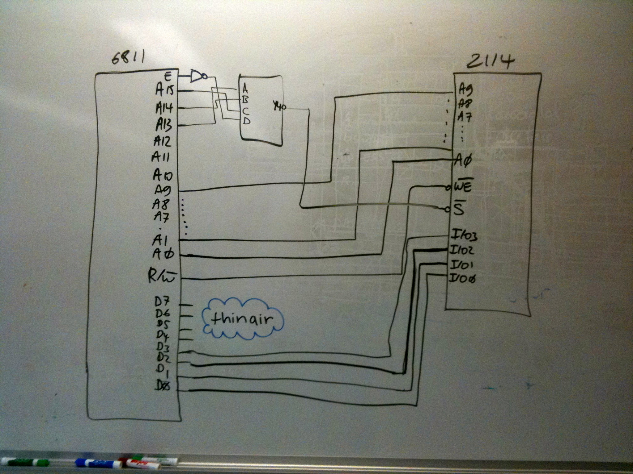
This lab is the last in the series of Circuits and Systems labs (the last lab will be with the Arduino board). You will interface a 2114 static RAM chip (SRAM) to the 6811.
You should have the 2114 datasheet that was handed out earlier.
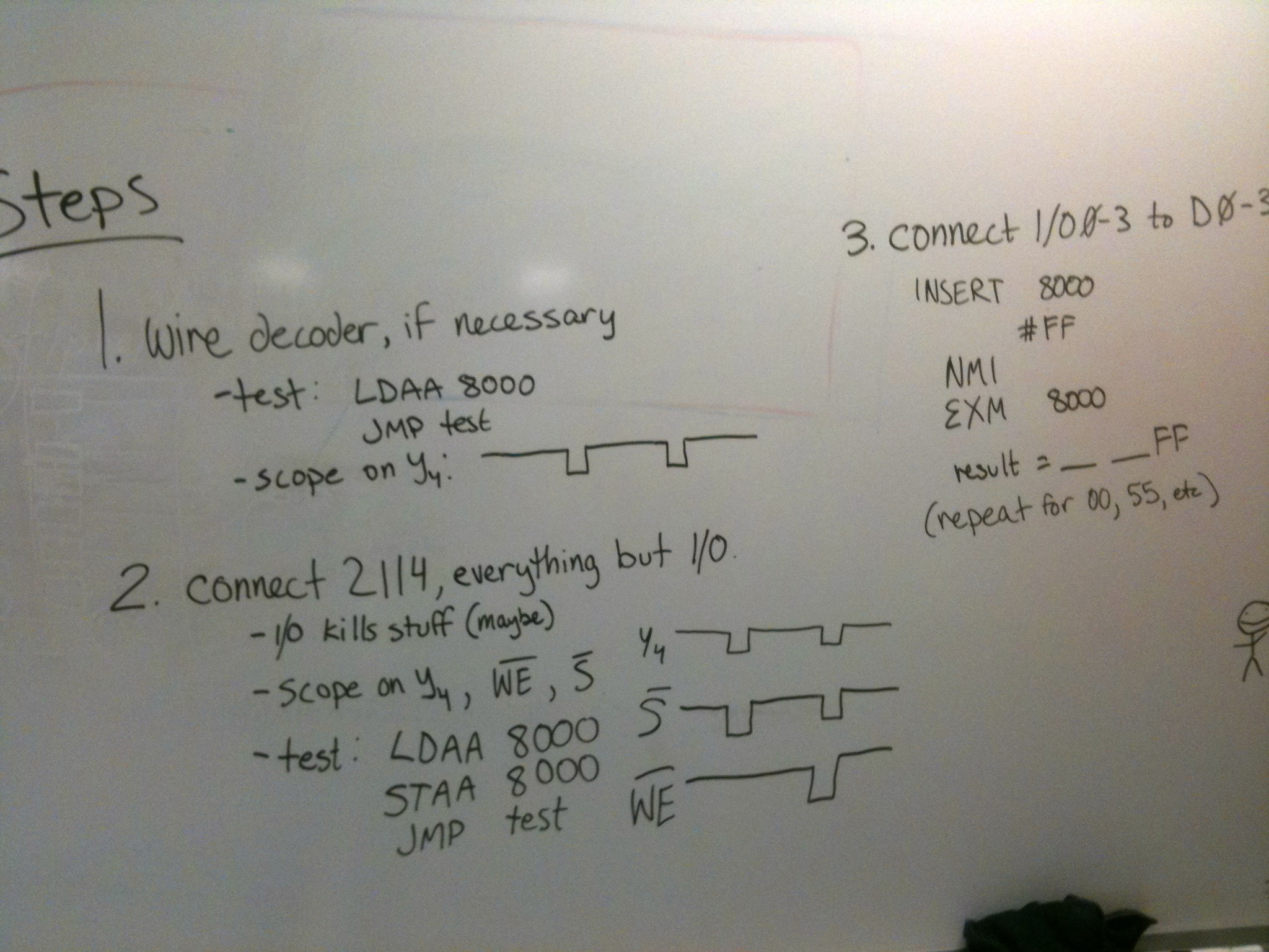
Today, your first job is to define a series of steps that must be taken so that:
- You wire up a 2114 (or two 2114s, if you are ambitious) and connect it/them to the 6811
- Do so in such a way that it is safe for the RAM and for the 6811. In other words, you have to define a series of steps in your wiring so that you can verify that all the signals behave correctly before making critical connections that could result in chips dying if the wiring is not done right.
- Define a way to verify and demonstrate that the RAM works as it should
In other words, you do all the work, including coming up with a real lab description!
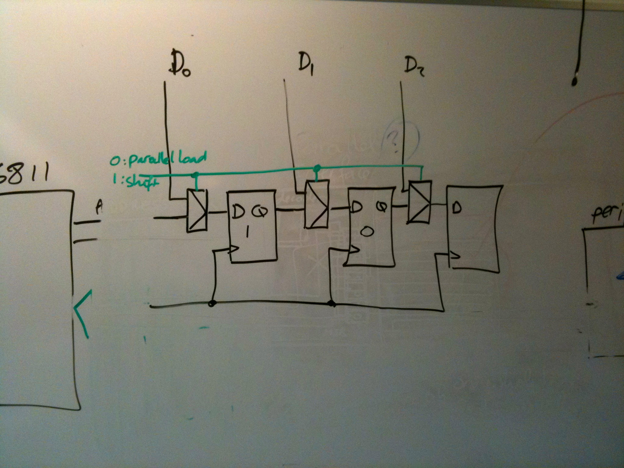
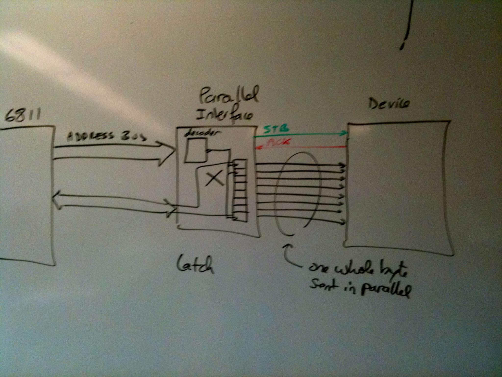
Board Snapshots (04/18/11 lecture)
Data Sheets


