Difference between revisions of "CSC270 Lab 0 2012"
(→EXPERIMENT #2: INTEGRATED CIRCUITS AND LOGIC GATES) |
|||
| Line 27: | Line 27: | ||
Explanations will be given in class. Our objective for today will be to design, implement, wire up, and demonstrate how a binary circuit works. | Explanations will be given in class. Our objective for today will be to design, implement, wire up, and demonstrate how a binary circuit works. | ||
| + | ===Overview of the Kit=== | ||
| + | <br /> | ||
| + | <center>[[Image:DigitalKit.jpg|700px]]</center> | ||
| + | <br /> | ||
| + | The main tools for us today are the switches, the LEDs, the +5 and GND wiring plots, and the breadboard area. | ||
| + | <br /> | ||
| + | ===Wiring=== | ||
We will refer to the diagram below for wiring integrated circuits. | We will refer to the diagram below for wiring integrated circuits. | ||
<br /> | <br /> | ||
| Line 47: | Line 54: | ||
<br /> | <br /> | ||
<br /> | <br /> | ||
| − | |||
=Useful Gates= | =Useful Gates= | ||
Revision as of 09:37, 27 January 2012
--D. Thiebaut 10:42, 25 January 2012 (EST)
Contents
Electronics Lab #0: Mini Lab to get the idea!
© D. Thiebaut, 2012
EXPERIMENT #1: INVESTIGATING THE KITt
For this part, concentrate only on the flatter part of the Digital Kit, not the circuit board that is upright, facing you. Please follow the steps below.
- Power OFF. Connect a wire between the Logic Indicator L4 and the Logic Switch A. Activate Switch A, and observe the LED (Light Emitting Diode) turn ON and OFF. Switch the wire from A to A-Bar, and see how the LED reacts .
- Power OFF. Same experiment, but this time replace the Logic Switch by one of the Data Switches.
- Power OFF. Connect one of the Logic Indicators to the Clock signal. Connect a second wire from another Logic Indicator to the Clock-bar signal. Make sure the sliding switch is on the 1Hz mark. Power UP. What do you observe?
- Slide the switch to 1KHz. What happens? Why? Is there any difference in the brightness of the LED? Why?
EXPERIMENT #2: INTEGRATED CIRCUITS AND LOGIC GATES
Explanations will be given in class. Our objective for today will be to design, implement, wire up, and demonstrate how a binary circuit works.
Overview of the Kit
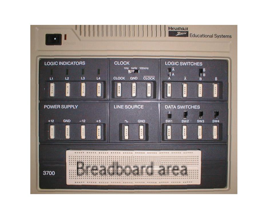
The main tools for us today are the switches, the LEDs, the +5 and GND wiring plots, and the breadboard area.
Wiring
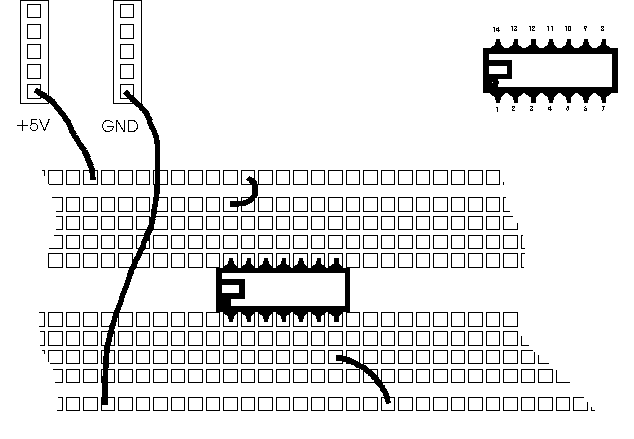
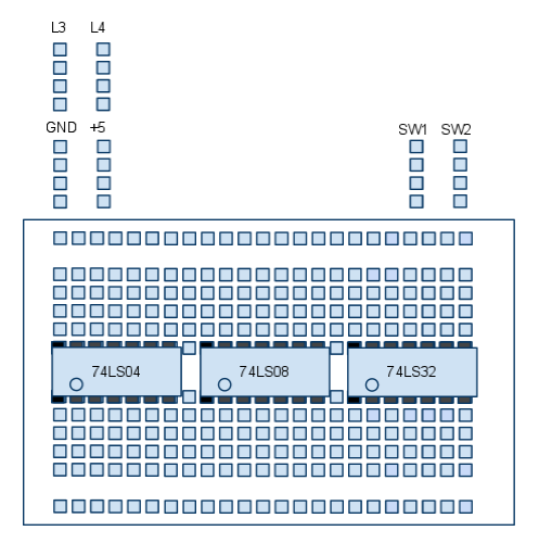
We will refer to the diagram below for wiring integrated circuits.
Figure 1: Wiring of an IC on the breadboard. Always identify pin 1 of the IC which is on the left (or below) the notch or circle embossed on the top of the chip
- Assume that we have two boolean variables, a and b. How could you prove that the following equality always hold?
a or (not a) and b = a or b
- We'll explore in class how to verify the property, both theoretically, on paper, and practically, using digital electronic circuits. The diagram below needs to be completed in class before wiring and testing.
Useful Gates
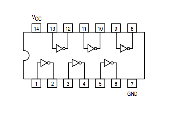
|
Inverter: 74LS04 | |
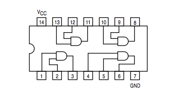
|
AND gate: 74LS08 | |
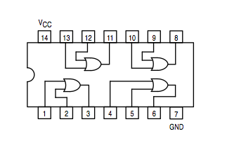
|
OR gate: 74LS32 | |
|
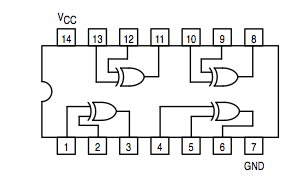
Exclusive OR: 74LS86 |
Data Sheets
If you need to refer to the data sheets of various chips during the lab, you can click on any of the links below: If the datasheets haven't been printed yet, print a set from these links: 74LS00 74LS01 74LS02 74LS03 74LS04 74LS05 74LS08 74LS09 74LS10 74LS12 74LS13 74LS15 74LS20 74LS21 74LS22 74LS26 74LS27 74LS28 74LS30 74LS32 74LS33 74LS37 74LS38 74LS40 74LS42 74LS47 74LS48 74LS51 74LS54 74LS55 74LS74 74LS75 74LS76 74LS83 74LS85 74LS86 74LS90 74LS9 74LS13 74HCT24 74LS24 74HCT24 74LS25 74HCT54.
3-Bit Adder (Optional)
- Write down all 8 possible binary results for the additions of 3 bits, and show the two bits that result: Carry and Sum, in a manner similar to the example below
    0
  + 0
  + 0
 ------
  X X
- Fill out the truth table below where a, b, and d are the three bits that are added together, C is the carry, and S the sum.
  a  b  d  |  Carry  Sum
-----------+--------------
  0  0  0  |
  0  0  1  |
  0  1  0  |
  0  1  1  |
  1  0  0  |
  1  0  1  |
  1  1  0  |
  1  1  1  |
- Generate the boolean expressions for C and S. This steps will require the whole class to work together! Keep on simplifying until you find an expression for S with only 2 operators, and an expression for C with only 5 operators!
- Generate the schematics for the circuit generating C and S
- Use the data sheets provided to assign pin numbers to the gates.
- Wire it up and demonstrate that you can correctly add 3 bits together!
