Difference between revisions of "Xilinx ISE Lab 2: Intro to Verilog"
(→New Source) |
(→Challenge #1) |
||
| (9 intermediate revisions by the same user not shown) | |||
| Line 13: | Line 13: | ||
<br /> | <br /> | ||
__TOC__ | __TOC__ | ||
| + | =Installation of Xilinx ISE 13.4 on Windows 7= | ||
| + | |||
| + | The first step is to install the ISE. It is a long process that can take more than an hour, so be prepared and start early! | ||
| + | |||
| + | Refer to the updated installation instructions that can be found [[Installing Xilinx ISE 13.4 on Win 7|here]]. | ||
| + | |||
=Introduction= | =Introduction= | ||
Xilinx's ISE is "Xilinx ISE[1] is a software tool produced by Xilinx for synthesis and analysis of HDL designs, which enables the developer to synthesize ("compile") their designs, perform timing analysis, examine RTL diagrams, simulate a design's reaction to different stimuli, and configure the target device with the programmer." <ref name="wiki_xilinx_ise">Xilinx ISE, captured on [http://en.wikipedia.org/wiki/Xilinx_ISE wikipedia.org], April 2012.</ref> | Xilinx's ISE is "Xilinx ISE[1] is a software tool produced by Xilinx for synthesis and analysis of HDL designs, which enables the developer to synthesize ("compile") their designs, perform timing analysis, examine RTL diagrams, simulate a design's reaction to different stimuli, and configure the target device with the programmer." <ref name="wiki_xilinx_ise">Xilinx ISE, captured on [http://en.wikipedia.org/wiki/Xilinx_ISE wikipedia.org], April 2012.</ref> | ||
| Line 21: | Line 27: | ||
This lab is based on the excellent series of labs created for the CoolRunner CPLD by Tiffany Liu in her Independent Study in the CS. Dept. at Smith College.<ref name="tiffanyLabs"> Tiffany Liu, ''CSC270 Labs on the CoolRunner-II'', Independent Study, Fall 2011, [http://cs.smith.edu/classwiki/index.php/CSC270_Labs_--_CSC400-Circuit_Design_F2011 cs.smith.edu/classwiki].</ref> | This lab is based on the excellent series of labs created for the CoolRunner CPLD by Tiffany Liu in her Independent Study in the CS. Dept. at Smith College.<ref name="tiffanyLabs"> Tiffany Liu, ''CSC270 Labs on the CoolRunner-II'', Independent Study, Fall 2011, [http://cs.smith.edu/classwiki/index.php/CSC270_Labs_--_CSC400-Circuit_Design_F2011 cs.smith.edu/classwiki].</ref> | ||
| − | |||
=Lab 2: Creating a 2-bit Adder in Verilog= | =Lab 2: Creating a 2-bit Adder in Verilog= | ||
| Line 71: | Line 76: | ||
* Name it with a name that makes sense, e.g. '''circuit2'''. | * Name it with a name that makes sense, e.g. '''circuit2'''. | ||
| − | * in the '''Define Module''' window, add '''A''' and '''B''' as inputs, and '''Sum''' and '''Carry''' as outputs. | + | * in the '''Define Module''' window, add '''A''' and '''B''' as <font color="magenta"> inputs</font>, and '''Sum''' and '''Carry''' as <font color="magenta">outputs</font>. |
* '''Finish''' | * '''Finish''' | ||
| Line 139: | Line 144: | ||
==Implementation Constraints File== | ==Implementation Constraints File== | ||
| − | + | Because we are not downloading the programming file to a device, we can skip the '''Implementation Constraints File''' creation step. | |
| − | |||
| − | |||
| − | |||
| − | |||
| − | |||
| − | |||
| − | |||
| − | |||
| − | |||
| − | |||
| − | |||
| − | |||
| − | |||
| − | |||
| − | |||
| − | |||
| − | |||
| − | |||
| − | |||
| − | |||
| − | |||
| − | |||
| − | |||
| − | |||
| − | |||
| − | |||
| − | |||
| − | |||
| − | |||
| − | |||
==Implement Design== | ==Implement Design== | ||
| − | |||
| − | |||
| − | |||
| − | |||
| − | |||
| − | * Select the ''' | + | * Select the '''circuit2.sch''' file in the '''Hierarchy''' window |
| − | * In the '''Process''' window, double click on '''Implement Desgin'''. This will automatically call all the actions listed above. The result is a programming file that will appear in the '' | + | * In the '''Process''' window, double click on '''Implement Desgin'''. This will automatically call all the actions listed above. The result is a programming file that will appear in the ''TwoBitAdderV'' project directory. |
| − | == | + | ==Testing the design with the simulator== |
| − | |||
| − | |||
| − | |||
| − | |||
This step will allow you to create a module that will make A and B take all the possible values ranging from 00, 01, 10, to 11, and see how the two-bit adder circuit reacts to it. | This step will allow you to create a module that will make A and B take all the possible values ranging from 00, 01, 10, to 11, and see how the two-bit adder circuit reacts to it. | ||
| Line 200: | Line 166: | ||
* the ISE will have generated a test module for us. It's almost what we need. We just need to modify it a tad, as shown below: | * the ISE will have generated a test module for us. It's almost what we need. We just need to modify it a tad, as shown below: | ||
| − | + | ||
| − | + | <source lang="verilog"> | |
| − | |||
| − | |||
| − | |||
| − | |||
| − | |||
| − | |||
| − | |||
| − | |||
| − | |||
| − | |||
| − | |||
| − | < | ||
| − | |||
| − | |||
`timescale 1ns / 1ps | `timescale 1ns / 1ps | ||
| − | module | + | //////////////////////////////////////////////////////////////////////////////// |
| + | // Company: | ||
| + | // Engineer: | ||
| + | // | ||
| + | // Create Date: 16:48:53 04/16/2012 | ||
| + | // Design Name: circuit2 | ||
| + | // Module Name: Y:[...] | ||
| + | // Project Name: TwoBittAdderV | ||
| + | // Target Device: | ||
| + | // Tool versions: | ||
| + | // Description: | ||
| + | // | ||
| + | // Verilog Test Fixture created by ISE for module: circuit2 | ||
| + | // | ||
| + | // Dependencies: | ||
| + | // | ||
| + | // Revision: | ||
| + | // Revision 0.01 - File Created | ||
| + | // Additional Comments: | ||
| + | // | ||
| + | //////////////////////////////////////////////////////////////////////////////// | ||
| − | + | module test; | |
| − | |||
| − | |||
| − | // | + | // Inputs |
| − | + | reg A; | |
| − | + | reg B; | |
| − | // | + | // Outputs |
| + | wire Carry; | ||
| + | wire Sum; | ||
| − | // Instantiate the UUT | + | // Instantiate the Unit Under Test (UUT) |
| − | + | circuit2 uut ( | |
| + | .A(A), | ||
| + | .B(B), | ||
.Carry(Carry), | .Carry(Carry), | ||
| − | .Sum(Sum) | + | .Sum(Sum) |
| − | + | ); | |
| − | + | ||
| − | + | initial begin | |
| − | + | // Initialize Inputs | |
| − | // Initialize Inputs | + | A = 0; |
| − | |||
| − | |||
B = 0; | B = 0; | ||
| − | |||
| − | // | + | // Wait 100 ns for global reset to finish |
| − | #100; | + | #100; |
| − | + | ||
| − | // | + | // Add stimulus here |
| − | + | #10 A = 1; | |
| − | + | #10 A = 0; B = 1; | |
| − | + | #10 A = 1; | |
| − | + | ||
| − | + | end | |
| − | + | ||
| − | |||
| − | |||
| − | |||
| − | |||
endmodule | endmodule | ||
| − | </ | + | |
| + | </source> | ||
<br /> | <br /> | ||
| Line 276: | Line 244: | ||
<br /> | <br /> | ||
| − | <center>[[Image: | + | <center>[[Image:Xilinx_ISim_Adder2.png|800px]]</center> |
<br /> | <br /> | ||
<br /> | <br /> | ||
| Line 285: | Line 253: | ||
===Challenge #1=== | ===Challenge #1=== | ||
|} | |} | ||
| − | [[Image: | + | [[Image:QuestionMark2.jpg|right|120px]] |
| − | * Use the same approach illustrated here and create a 3-bit adder. | + | * Use the same approach illustrated here and create a 3-bit adder. For this exercise, you can either define the two output bits in terms of their boolean equations of the tree inputs, or as being the actual sum of three bits. For the first approach you would define '''Sum''' as follows: |
| + | |||
| + | assign Sum = a ^ b ^ Cin; | ||
| + | |||
| + | :and you would define Cout using the appropriate boolean equation. | ||
| + | |||
| + | |||
| + | assign Cout = // you figure it out! | ||
| + | |||
| + | : For the second approach, though, you can simply express that Cout, Sum represent the sum of three bits: | ||
| + | |||
| + | assign {Cout, Sum} = a + b + Cin; | ||
| + | |||
| + | :Try both approaches! | ||
| + | |||
<br /> | <br /> | ||
<br /> | <br /> | ||
Latest revision as of 11:36, 22 April 2012
--D. Thiebaut 16:37, 16 April 2012 (EDT)
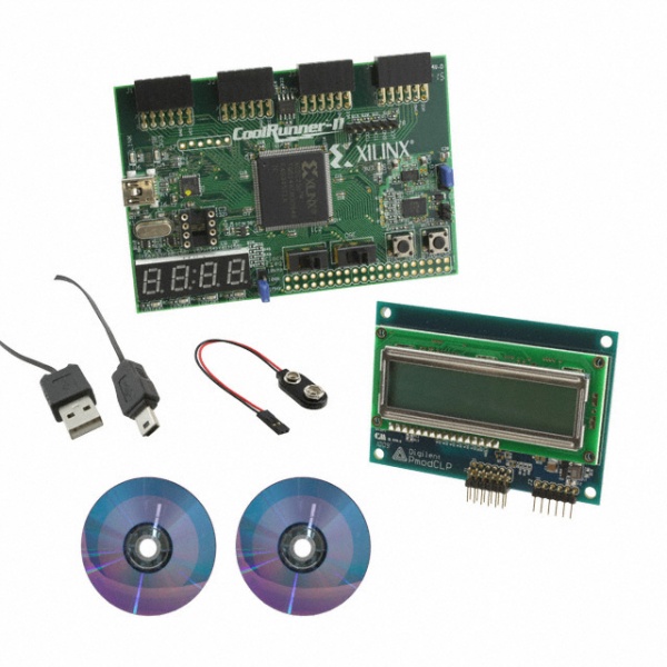
This lab is the second lab introducing the Xilinx ISE and to the CoolRunner-II kit. Make sure you do Lab #1 of this series first.
This lab will show you how to create a two-bit adder in Verilog and check its correct operation with the ISim simulator.

Contents
Installation of Xilinx ISE 13.4 on Windows 7
The first step is to install the ISE. It is a long process that can take more than an hour, so be prepared and start early!
Refer to the updated installation instructions that can be found here.
Introduction
Xilinx's ISE is "Xilinx ISE[1] is a software tool produced by Xilinx for synthesis and analysis of HDL designs, which enables the developer to synthesize ("compile") their designs, perform timing analysis, examine RTL diagrams, simulate a design's reaction to different stimuli, and configure the target device with the programmer." [1]
The goal of this lab/tutorial is to get the reader familiar with the process of designing a simple digital electronic circuit, compiling it, and verifying it correct behavior with a simulator.
Knowledge of digital logic (basic gates, flip-flops, Moore machines) is assumed.
This lab is based on the excellent series of labs created for the CoolRunner CPLD by Tiffany Liu in her Independent Study in the CS. Dept. at Smith College.[2]
Lab 2: Creating a 2-bit Adder in Verilog
New Project
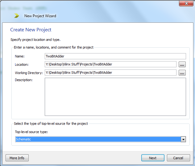
- Open the ISE
- File/New Project
- Pick a name: TwoBitAdderV
- Accept the default location
- Top-Level source: HDL
- Project Settings:
- Family: CoolRunner2 CPLDs
- Device: XC2C257 (this is the marking on the CPLD on the actual kit)
- Package: TQ144 (also marked on the CPLD on the actual kit)
- Speed: -7
- Keep all others unchanged.
New Source
- Click on top left icon (see image to the right) to add a new source to the project.
- Pick Verilog Module as the type
- Name it with a name that makes sense, e.g. circuit2.
- in the Define Module window, add A and B as inputs, and Sum and Carry as outputs.
- Finish
- You should then see the following template ready for you to complete:
`timescale 1ns / 1ps
//////////////////////////////////////////////////////////////////////////////////
// Company:
// Engineer:
//
// Create Date:    16:36:46 04/16/2012
// Design Name:
// Module Name:    circuit2
// Project Name:
// Target Devices:
// Tool versions:
// Description:
//
// Dependencies:
//
// Revision:
// Revision 0.01 - File Created
// Additional Comments:
//
//////////////////////////////////////////////////////////////////////////////////
module circuit2(
    input A,
    input B,
    output Carry,
    output Sum
    );


endmodule
- Edit the Verilog file, and add just to lines:
module circuit2(
    input A,
    input B,
    output Carry,
    output Sum
    );

	and( Carry, A, B );
	xor( Sum, A, B );

endmodule
- Type Control-S to save the Verilog code to file.
Implementation Constraints File
Because we are not downloading the programming file to a device, we can skip the Implementation Constraints File creation step.
Implement Design
- Select the circuit2.sch file in the Hierarchy window
- In the Process window, double click on Implement Desgin. This will automatically call all the actions listed above. The result is a programming file that will appear in the TwoBitAdderV project directory.
Testing the design with the simulator
This step will allow you to create a module that will make A and B take all the possible values ranging from 00, 01, 10, to 11, and see how the two-bit adder circuit reacts to it.
- First create a new simulation module: From the main menu, pick Project then New Source.
- Choose Verilog Test Fixture as the type of the module. Give it a meaningful name, for example test.
- Click Next and make sure that your original schematic module is selected.
- Next then Finish.
- the ISE will have generated a test module for us. It's almost what we need. We just need to modify it a tad, as shown below:
`timescale 1ns / 1ps

////////////////////////////////////////////////////////////////////////////////
// Company:
// Engineer:
//
// Create Date:   16:48:53 04/16/2012
// Design Name:   circuit2
// Module Name:   Y:[...]
// Project Name:  TwoBittAdderV
// Target Device:
// Tool versions:
// Description:
//
// Verilog Test Fixture created by ISE for module: circuit2
//
// Dependencies:
//
// Revision:
// Revision 0.01 - File Created
// Additional Comments:
//
////////////////////////////////////////////////////////////////////////////////

module test;

	// Inputs
	reg A;
	reg B;

	// Outputs
	wire Carry;
	wire Sum;

	// Instantiate the Unit Under Test (UUT)
	circuit2 uut (
		.A(A),
		.B(B),
		.Carry(Carry),
		.Sum(Sum)
	);

	initial begin
		// Initialize Inputs
		A = 0;
		B = 0;

		// Wait 100 ns for global reset to finish
		#100;

		// Add stimulus here
                #10  A = 1;
                #10 A = 0; B = 1;
                #10   A = 1;

	end

endmodule
- Click on the Simulation button on top of the Hierarchy pane.
- The ISim Simulator should appear in the Process pane, below.
- Double click on Behavioral Check Syntax
- Then, assuming the process completed successfully, double click on Simulate Behavioral Model
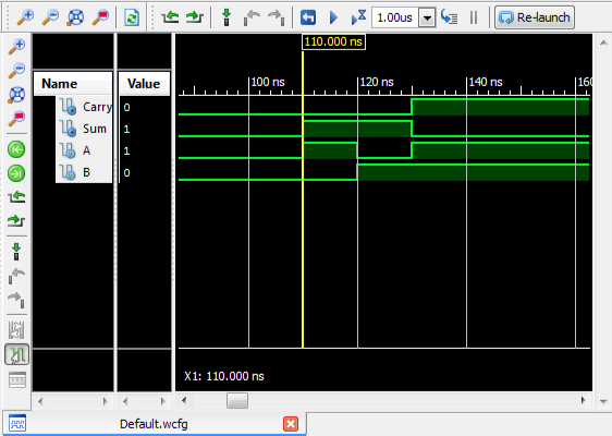
- A new window should open up, presenting a timing diagram. Use slider and the magnifying glass + and - icons to zoom in on the marker at Time 100ns, and see how Sum and Carry react to the changing A and B signals.
- Make sure you verify that the adder works correctly.

Challenge #1 |
- Use the same approach illustrated here and create a 3-bit adder. For this exercise, you can either define the two output bits in terms of their boolean equations of the tree inputs, or as being the actual sum of three bits. For the first approach you would define Sum as follows:
assign Sum = a ^ b ^ Cin;
- and you would define Cout using the appropriate boolean equation.
assign Cout = // you figure it out!
- For the second approach, though, you can simply express that Cout, Sum represent the sum of three bits:
assign {Cout, Sum} = a + b + Cin;
- Try both approaches!
References
- ↑ Xilinx ISE, captured on wikipedia.org, April 2012.
- ↑ Tiffany Liu, CSC270 Labs on the CoolRunner-II, Independent Study, Fall 2011, cs.smith.edu/classwiki.

