Difference between revisions of "Xilinx ISE Four-Bit Adder in Verilog"
(→Simulation) |
|||
| Line 230: | Line 230: | ||
* Verify that you obtain a timing diagram that demonstrates the correct operation of your adder: | * Verify that you obtain a timing diagram that demonstrates the correct operation of your adder: | ||
| − | <br /><center>[[Image:Xilinx_Verilog_FullAdder_Simulation_Timing.png]]</center> | + | <br /><center>[[Image:Xilinx_Verilog_FullAdder_Simulation_Timing.png|700px]]</center> |
<br /> | <br /> | ||
Revision as of 13:13, 24 April 2012
--D. Thiebaut 11:03, 24 April 2012 (EDT)
This lab should be done after the introduction lab on Verilog. It shows how to use two modules, one for the basic 3-bit full-adder (adding a to b with carry-in), and one that uses 4 of them to create a 4-bit adder with an output carry.
Contents
Full-Adder in Verilog
Review
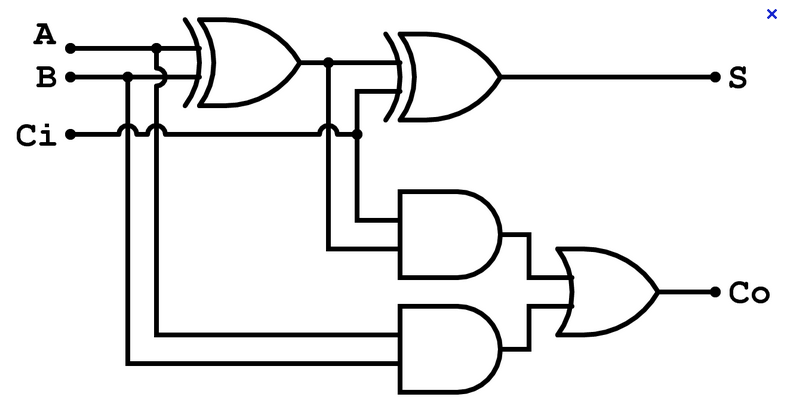
A full adder is a combinational logic that takes 3 bits, a, b, and carry-in, and outputs their sum, in the form of two bits, carry-out, and sum.
The figure below illustrates the circuit:

New Project
- The first task is start the Xilinx ISE and create a New Project. Let's call it FourBitAdder.
- Once the Project is created, add a New Source, of type Verilog Module. Call it MultiStages. It will contain 2 modules. The first one will be the 3-bit full adder.
- Define the ports as follows:
- a, input
- b, input
- cin, input
- s, output
- cout, output
We now have several options to define the adder. One is functional, as illustrated in the next subsection. Next is a logical description, where we express the outputs in terms of their logical equation. The final is a gate level description. Pick the one that seem most interesting to you. They should all yield the same result in the next section, where we test them.
Functional Description of Full Adder
`timescale 1ns / 1ps
//////////////////////////////////////////////////////////////////////////////////
// MultiStages.v
//
//////////////////////////////////////////////////////////////////////////////////
module singleStage (
	 input a,
	 input b,
	 input cin,
	 output s,
	 output cout );

	assign {cout,s} = a + b + cin;

endmodule

module MultiStages(
    input [3:0] a,
    input [3:0] b,
    output [3:0] sum,
    output carry
    );

endmodule
Logical Description of Full Adder
- Complete the code of the module so that it looks like this:
`timescale 1ns / 1ps
//////////////////////////////////////////////////////////////////////////////////
// MultiStages.v
//
//////////////////////////////////////////////////////////////////////////////////
module singleStage (
	 input a,
	 input b,
	 input cin,
	 output s,
	 output cout );

         assign s = a ^ b ^ cin;
	 assign cout = (a & b)  |  (a & cin)  |  (b & cin);

endmodule

module MultiStages(
    input [3:0] a,
    input [3:0] b,
    output [3:0] sum,
    output carry
    );

endmodule
Gate-Level Description of Full Adder
`timescale 1ns / 1ps
//////////////////////////////////////////////////////////////////////////////////
// MultiStages.v
//
//////////////////////////////////////////////////////////////////////////////////
module singleStage (
	 input a,
	 input b,
	 input cin,
	 output s,
	 output cout );

         // wires (from ands to or)
	 wire w1, w2, w3;

         // carry-out circuitry
	 and( w1, a, b );
	 and( w2, a, cin );
	 and( w3, b, cin );
	 or( cout, w1, w2, w3 );

         // sum
	 xor( s, a, b, cin );

endmodule


module MultiStages(
    input [3:0] a,
    input [3:0] b,
    output [3:0] sum,
    output carry
    );

endmodule
Check Module for Syntax Errors
- Click on the module file and select it in the Implementation window, and
- In the Process window, below the implementation window, double click on Synthesize, in the Implement Design menu.
- You should get this message in the console:
Process "Simulate Behavioral Model" completed successfully
- (If not, fix the bugs and retry!)
Generate a Test Module
- Add a New Source to the project, of type Verilog Test Fixture.
- Call it test.
- Specify singleStage as the target of the testing (be careful there will be two targets as you have two modules in your main file).
- Edit the test.v file as illustrated below:
`timescale 1ns / 1ps

////////////////////////////////////////////////////////////////////////////////
// Module Name:   Y:/Desktop/Xilinx Stuff/Projects/NBitAdder/test.v
//
////////////////////////////////////////////////////////////////////////////////

module test;

	// Inputs
	reg a;
	reg b;
	reg cin;

	// Outputs
	wire s;
	wire cout;

	integer i;

	// Instantiate the Unit Under Test (UUT)
	singleStage uut (
		.a(a),
		.b(b),
		.cin(cin),
		.s(s),
		.cout(cout)
	);

	initial begin
		// Initialize Inputs
		a = 0;
		b = 0;
		cin = 0;
	end

	always @ ( a, b, cin )
		begin

                // generate truth table
		for ( i = 0; i < 8; i = i + 1 )
                        // every 10 ns set a, b, and cin to the binary rep. of i
			#10 {a, b, cin} = i;

                // stop 10ns after last change of inputs
		#10 $stop;
		end


endmodule
Some explanations
- integer i
- this is necessary since we have a loop that is going 8 times
- initial begin
- an initial block is done only once, at the beginning of the simulation. Here we make sure all the signals are 0 when we start.
- always @ ( a or b or cin )
- an always block means that whenever a or b or cin are modified the inside of the block should be evaluated. In essence we mean that whatever is in this block is dynamic and should be evaluated at any signal change.
- #10 {a, b, cin} = i
- After a delay of 10 ns, we take the bits that form the integer i (by default an integer contains 32 bits) and assign the lower ones to the three bits a, b, and cin. It's an easy way to generate a truth table.
- #10 $stop
- 10 ns after the loop has terminated, stop the simulation.
Simulation
- Click on the Simulation button at the top of the Design Window,
- Select test.v as target
- Click on Behavioral Check Syntax and fix any bugs you may have.
- Finally, double click on Simulate Behavioral Model
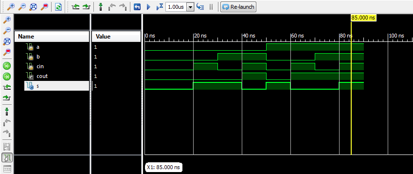
- Verify that you obtain a timing diagram that demonstrates the correct operation of your adder:
