Difference between revisions of "CSC270 Homework 5 2016"
(Created page with "--~~~~ ---- =Problem 1= <br /> 500px|center <br />") |
|||
| Line 6: | Line 6: | ||
[[Image:Homework5Sequencer1.png|500px|center]] | [[Image:Homework5Sequencer1.png|500px|center]] | ||
<br /> | <br /> | ||
| + | ==Part 1== | ||
| + | <br /> | ||
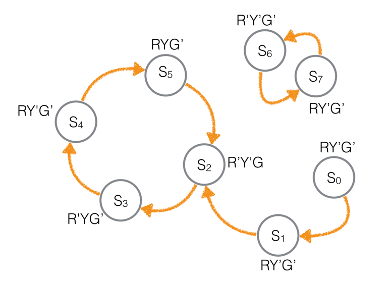
| + | * The timing diagram above is that of a sequencer. Notice that when it starts in States S6 or S7, it keeps oscillating between the two states. If it starts on any of S2, S3, S4, or S5, it cycles through the states, endlessly. If it starts in S0 or S1, it eventually gets to the 4-state cycle. | ||
| + | * Your assignment is to design this sequencer with D Flip-flops. | ||
| + | * Your design should show the transition table containing the Q outputs, and the GYR outputs. | ||
| + | * Your design should also contain a Python program showing that you were able to fully test that your boolean equations actually make the sequencer operate with the same state diagram as the one shown above. | ||
| + | * Include the Python code, and its output or outputs (you need to show that the sequencer works correctly, no matter what state it starts in. | ||
| + | <br /> | ||
| + | ==Part 2== | ||
| + | <br /> | ||
| + | * Obviously, the original designer of this sequencer did not intend for the sequencer to get stuck in the S6-S7 cycle. | ||
| + | * Recommend as cheap a fix as possible, so that if the sequencer starts in S6 or S7, it automatically ends up in the S2, S3, S4, S5 cycle. You are free to connect the two independent graphs whichever way you want. | ||
| + | ::A cheap fix is one that requires as few extra gates as possible. If your fix requires one additional inverter, then we'll count your fix as worth 1/6, since there are 6 inverters in a 7404 IC. If your fix requires an addition AND, OR, XOR, NAND, or NOR, then your fix will be worth 1/4. If your fix requires removing 3 gates and adding a 7442 decoder, for example, then your fix would be -3/4 + 1/1 = 1/4. | ||
| + | * Explain how your fix works, and indicate its cost. | ||
| + | <br /> | ||
| + | <br /> | ||
| + | <br /> | ||
| + | <br /> | ||
| + | <br /> | ||
| + | <br /> | ||
| + | <br /> | ||
| + | <br /> | ||
| + | <br /> | ||
| + | <br /> | ||
| + | <br /> | ||
| + | <br /> | ||
| + | <br /> | ||
| + | <br /> | ||
| + | [[Category:CSC270]][[Category:Homework]] | ||
Revision as of 21:01, 24 February 2016
--D. Thiebaut (talk) 19:34, 24 February 2016 (EST)
Problem 1
Part 1
- The timing diagram above is that of a sequencer. Notice that when it starts in States S6 or S7, it keeps oscillating between the two states. If it starts on any of S2, S3, S4, or S5, it cycles through the states, endlessly. If it starts in S0 or S1, it eventually gets to the 4-state cycle.
- Your assignment is to design this sequencer with D Flip-flops.
- Your design should show the transition table containing the Q outputs, and the GYR outputs.
- Your design should also contain a Python program showing that you were able to fully test that your boolean equations actually make the sequencer operate with the same state diagram as the one shown above.
- Include the Python code, and its output or outputs (you need to show that the sequencer works correctly, no matter what state it starts in.
Part 2
- Obviously, the original designer of this sequencer did not intend for the sequencer to get stuck in the S6-S7 cycle.
- Recommend as cheap a fix as possible, so that if the sequencer starts in S6 or S7, it automatically ends up in the S2, S3, S4, S5 cycle. You are free to connect the two independent graphs whichever way you want.
- A cheap fix is one that requires as few extra gates as possible. If your fix requires one additional inverter, then we'll count your fix as worth 1/6, since there are 6 inverters in a 7404 IC. If your fix requires an addition AND, OR, XOR, NAND, or NOR, then your fix will be worth 1/4. If your fix requires removing 3 gates and adding a 7442 decoder, for example, then your fix would be -3/4 + 1/1 = 1/4.
- Explain how your fix works, and indicate its cost.
