Difference between revisions of "CSC270 Lab 9 2012"
(→Testing your circuit) |
(→A software driver) |
||
| (10 intermediate revisions by the same user not shown) | |||
| Line 1: | Line 1: | ||
--[[User:Thiebaut|D. Thiebaut]] 11:25, 10 April 2012 (EDT) | --[[User:Thiebaut|D. Thiebaut]] 11:25, 10 April 2012 (EDT) | ||
---- | ---- | ||
| − | |||
| − | |||
| − | |||
<bluebox> | <bluebox> | ||
This lab will take you through the steps required to build a 1-bit '''output port''' with the 6811 Kit. | This lab will take you through the steps required to build a 1-bit '''output port''' with the 6811 Kit. | ||
</bluebox> | </bluebox> | ||
| + | |||
| + | __TOC__ | ||
| + | |||
| + | <!--center>Motto for the lab today:<br /> ''Less is More'', also known as Occam's razor.</center--> | ||
| + | =Background= | ||
| + | |||
| + | Everything you are doing today must somehow refer to this diagram for validity. So make sure you understand it and can extract from it the basic ''rules'' followed by a processor when it accesses memory. | ||
| + | <br /> | ||
| + | <br /> | ||
| + | <center>[[Image:CSC270 FigureA14.png|400px]]</center> | ||
<br /> | <br /> | ||
| − | + | ||
=I/O Address= | =I/O Address= | ||
| Line 61: | Line 68: | ||
=Testing your circuit= | =Testing your circuit= | ||
| − | [[Image:CSC270_6811_IO3.png| | + | [[Image:CSC270_6811_IO3.png|400px|right]] |
Wire up your circuit. Make sure you put the 7442 in the leftmost section of the breadboard, as you will be reusing it in the next lab(s). For this reason make sure you keep the 7442 wired up on the breadboad at the end of today's lab, so you won't have to rewire it next time when we wire up an input port. | Wire up your circuit. Make sure you put the 7442 in the leftmost section of the breadboard, as you will be reusing it in the next lab(s). For this reason make sure you keep the 7442 wired up on the breadboad at the end of today's lab, so you won't have to rewire it next time when we wire up an input port. | ||
| Line 70: | Line 77: | ||
Verify that you see something like the picture on the right, taken by Tiffany Liu: | Verify that you see something like the picture on the right, taken by Tiffany Liu: | ||
| − | + | ||
In your report, explain which signal is which, and why this timing diagram is the correct one. Make sure the scale is clear, especially the time scale. In particular, indicate where your endless loop starts and ends, and how long it lasts. Relate that to the number of cycles your endless loop is supposed to take. | In your report, explain which signal is which, and why this timing diagram is the correct one. Make sure the scale is clear, especially the time scale. In particular, indicate where your endless loop starts and ends, and how long it lasts. Relate that to the number of cycles your endless loop is supposed to take. | ||
| − | [[IMage:CSC270_6811_IO2.png| | + | [[IMage:CSC270_6811_IO2.png| 400px|right]] |
Now add a scope probe to the Q output of the flipflop. This is the bit that you are storing in the 1-bit I/O Port which your flipflop implements. | Now add a scope probe to the Q output of the flipflop. This is the bit that you are storing in the 1-bit I/O Port which your flipflop implements. | ||
| − | Verify that you see something like the one on the right, taken | + | Verify that you see something like the one on the right, taken by Tiffany Liu. |
In your report, explain which signal is which, and why this timing diagram is the correct one. | In your report, explain which signal is which, and why this timing diagram is the correct one. | ||
| Line 102: | Line 109: | ||
Here is a way to organize your endless loop using these functions: | Here is a way to organize your endless loop using these functions: | ||
| + | <br /> | ||
| + | <source lang="text"> | ||
LED EQU ???? ; enter the address energizing your Yi output | LED EQU ???? ; enter the address energizing your Yi output | ||
| Line 117: | Line 126: | ||
staa LED | staa LED | ||
rts | rts | ||
| − | + | </source> | |
| + | <br /> | ||
The '''JSR''' and '''RTS''' instructions are new. The JSR instruction '''J'''umps to a '''S'''ub'''R'''outine which is another name for function. It is like a jump except the processor also saves in the stack the address it must return to in the main program when it encounters the RTS instruction. RTS means '''R'''re'''T'''urn from '''S'''ubroutine, and it will pop off the stack the return address and put it in the Program Counter. | The '''JSR''' and '''RTS''' instructions are new. The JSR instruction '''J'''umps to a '''S'''ub'''R'''outine which is another name for function. It is like a jump except the processor also saves in the stack the address it must return to in the main program when it encounters the RTS instruction. RTS means '''R'''re'''T'''urn from '''S'''ubroutine, and it will pop off the stack the return address and put it in the Program Counter. | ||
| Line 124: | Line 134: | ||
=Slowing down the loop= | =Slowing down the loop= | ||
| − | The table below shows entry points in the ''Monitor'' (that's the name of the tiny operating system of the kit) for doing different things, like reading characters, displaying strings, etc. One of them is the entry point for a wait subroutine that is a delay of 1 second. When you jump to this address with a JSR instruction, you will return to your program only after a 1 second delay. | + | The table below is familiar by now. You saw it in a recent homework assignment. It shows entry points in the ''Monitor'' (that's the name of the tiny operating system of the kit) for doing different things, like reading characters, displaying strings, etc. One of them is the entry point for a wait subroutine that is a delay of 1 second. When you jump to this address with a JSR instruction, you will return to your program only after a 1 second delay. |
| − | ::''Note: Be careful about the JSR Delay call: it will not maintain the value that is in Acca when you call it. So if you expect Acca to have the same value when you return from the Delay subroutine, put it in a variable before the call, and get it back from the variable after the call. You can also push it in the stack and pop it from the stack before and after the call; that will work too!'' | + | ::''Note: Be careful about the JSR Delay call: it will not maintain the value that is in '''Acca''' when you call it. So if you expect Acca to have the same value when you return from the Delay subroutine, put it in a variable before the call, and get it back from the variable after the call. You can also push it in the stack and pop it from the stack before and after the call; that will work too!'' |
Add calls to the delay subroutine in your loop so that we can see your LED stay ON for a second, then turn OFF for a second, and so on. | Add calls to the delay subroutine in your loop so that we can see your LED stay ON for a second, then turn OFF for a second, and so on. | ||
| Line 136: | Line 146: | ||
=Questions= | =Questions= | ||
| − | + | Include the answer to these questions in your report | |
* '''Question 1''': What is the frequency at which your LED blink (without the delay routine)? | * '''Question 1''': What is the frequency at which your LED blink (without the delay routine)? | ||
| Line 150: | Line 160: | ||
Since we now know how to build a 1-bit output port, and since the 74LS74 contains 2 flip-flops, create a 2-bit output port, with the''' least amount''' of additional hardware. | Since we now know how to build a 1-bit output port, and since the 74LS74 contains 2 flip-flops, create a 2-bit output port, with the''' least amount''' of additional hardware. | ||
| − | + | '''Make sure to run your design by me''' before wiring it up. | |
When your design is approved, demonstrate that your 2-bit port works by making the two LEDs count in binary (00, 01, 10, 11, 00, etc.) Make your code '''as simple''' as possible! | When your design is approved, demonstrate that your 2-bit port works by making the two LEDs count in binary (00, 01, 10, 11, 00, etc.) Make your code '''as simple''' as possible! | ||
Latest revision as of 15:21, 29 March 2016
--D. Thiebaut 11:25, 10 April 2012 (EDT)
This lab will take you through the steps required to build a 1-bit output port with the 6811 Kit.
Contents
Background
Everything you are doing today must somehow refer to this diagram for validity. So make sure you understand it and can extract from it the basic rules followed by a processor when it accesses memory.

I/O Address
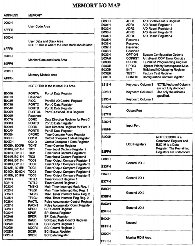
First you need to find a range of addresses that are not used for RAM, ROM or I/O devices by the 6811 in the Heathkit. Get the handout showing the memory address map for the kit and pick one address that will not energize memory or already-built I/O devices.
Setup
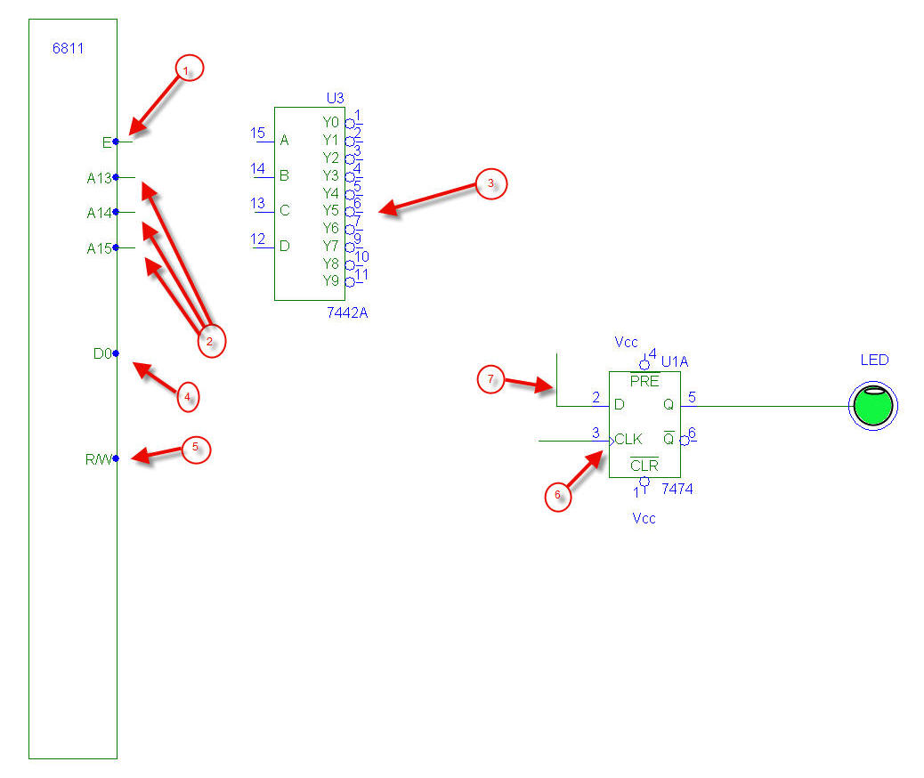
The figure below contains all the main players for today's lab.
You have to figure out the missing areas, with a little bit of help:
- 1. E. The clock. You are going to use it to make the decoder operate only during the second half of a processor cycle, when all the signals are stable. E is low in the first half of the cycle, and is high in the second half.
- A decoder used as "logic glue" is a good way to connect a processor to devices such as memory or I/O devices. One problem, though, is that the 7442 decoder that we have available to us is a 4-to-10 decoder that does not have an Enable input... We'll have to work with that...
- 2. The Address bits A15, A14, A13. Somehow we should connect them along with E to the decoder so that we can recognize an address in the range 7000 to AFFF (which we should have discovered in the first part of this lab to be available to us, since we don't have a memory cartridge installed in the kit).
Figure out a way to connect E, A15, A14, and A13 to the decoder inputs so that one of the Yi outputs is activated for an address that you will have selected in the range 7000 to AFFF, and only in the second half of the E cycle. Make sure that the Y output you selected is not activated by any address lower than 7000, or by an address higher than AFFF.
                        address                  Yi activated by this address
                        ________                 _____________________________

                        6000 (RAM)                   Y_

                        7000 (avail)                 Y_

                        8000 (avail)                 Y_

                        9000 (avail)                 Y_

                        A000 (µP IO)                 Y_
- 3. There isn't one unique answer for the selection of Yi output. Depending on how you connect the A15, A14, A13 and E signals to the decoder, you may end up with a Yi that is not the same as the Yi another team will have selected during this lab. You now need to use the Yi active-low output that you have selected and see how it should be connected to the clock input of the D-flipflop.
- Complete the timing diagram below showing the shape of the different signals when the processor is writing at the address you selected as the address of your I/O device.
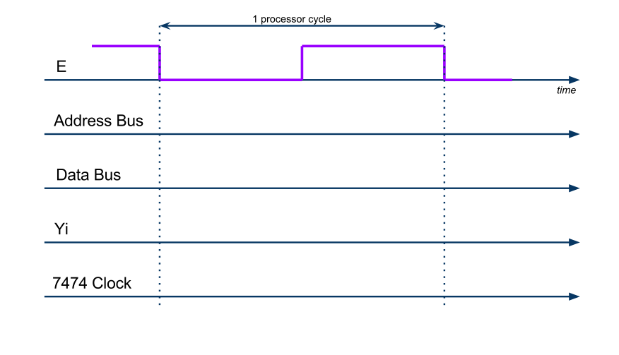
- 4. This step should be straightforward. Connect the D0 output of the data bus to the data input of your flipflop...
- 5. This step should have been taken care of in Step 4 above. Make sure you get me to verify your schematics before you start wiring things up.
Testing your circuit
Wire up your circuit. Make sure you put the 7442 in the leftmost section of the breadboard, as you will be reusing it in the next lab(s). For this reason make sure you keep the 7442 wired up on the breadboad at the end of today's lab, so you won't have to rewire it next time when we wire up an input port.
Write a simple endless loop that repeatedly write 0, then 1, then 0, then 1, etc., to your 1-bit flipflop. Assemble it, enter it in the kit, and run it.
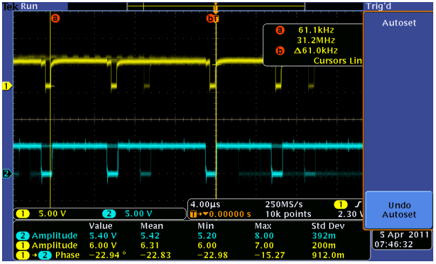
Use the scope and take a look at R/W and your Yi output.
Verify that you see something like the picture on the right, taken by Tiffany Liu:
In your report, explain which signal is which, and why this timing diagram is the correct one. Make sure the scale is clear, especially the time scale. In particular, indicate where your endless loop starts and ends, and how long it lasts. Relate that to the number of cycles your endless loop is supposed to take.
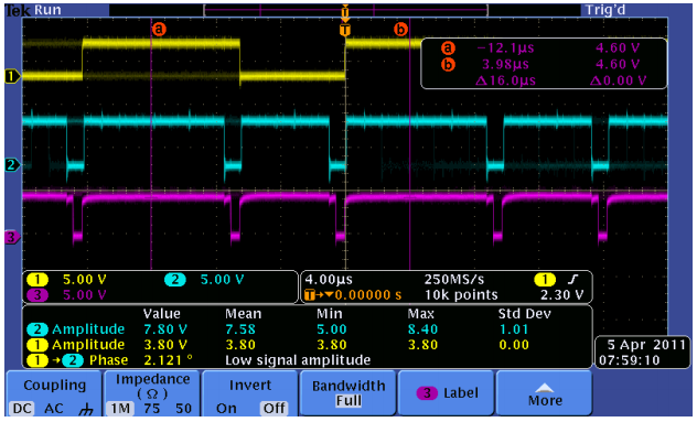
Now add a scope probe to the Q output of the flipflop. This is the bit that you are storing in the 1-bit I/O Port which your flipflop implements.
Verify that you see something like the one on the right, taken by Tiffany Liu.
In your report, explain which signal is which, and why this timing diagram is the correct one.
A software driver
A simple way to write a driver is to create two functions that can be called to set the LED ON, or to turn it OFF.
We can call the first function turnLEDOn, and the second one turnLEDOff.
Here is a way to organize your endless loop using these functions:
      LED        EQU        ????         ; enter the address energizing your Yi output

                 ORG        0000
      loop:      jsr        turnLEDOn
                 jsr        turnLEDOff
                 jmp        loop

                 ORG        0010
      turnLEDOn: ldaa       #1
                 staa       LED
                 rts

      turnLEDOff:ldaa       #0
                 staa       LED
                 rts
The JSR and RTS instructions are new. The JSR instruction Jumps to a SubRoutine which is another name for function. It is like a jump except the processor also saves in the stack the address it must return to in the main program when it encounters the RTS instruction. RTS means RreTurn from Subroutine, and it will pop off the stack the return address and put it in the Program Counter.
Assemble the above program by hand, and verify that you get a similar waveform as the last one you got before, where the time scale may have changed (why?).
Slowing down the loop
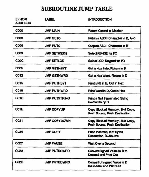
The table below is familiar by now. You saw it in a recent homework assignment. It shows entry points in the Monitor (that's the name of the tiny operating system of the kit) for doing different things, like reading characters, displaying strings, etc. One of them is the entry point for a wait subroutine that is a delay of 1 second. When you jump to this address with a JSR instruction, you will return to your program only after a 1 second delay.
- Note: Be careful about the JSR Delay call: it will not maintain the value that is in Acca when you call it. So if you expect Acca to have the same value when you return from the Delay subroutine, put it in a variable before the call, and get it back from the variable after the call. You can also push it in the stack and pop it from the stack before and after the call; that will work too!
Add calls to the delay subroutine in your loop so that we can see your LED stay ON for a second, then turn OFF for a second, and so on.
Questions
Include the answer to these questions in your report
- Question 1: What is the frequency at which your LED blink (without the delay routine)?
- Question 2: What is the fastest frequency at which you can make the LED blink? Please answer with a theoretical answer, which includes the frequency of E, and what you know of 6811 instructions, and how you can arrange them to allow for the fastest possible way to switch the LED On and Off repeatedly.
- Question 3: Once you stored a bit in the flip-flop, can you read it back from your program. In other words, assume you want your program to discover what the value of the output Q of the flipflop is, can your program do it, and if so, how?
- Question 4: Can you use the keyboard to store 1 or 0 in your 1-bit port? Try it. What do you observe?
Two-bit Port
Since we now know how to build a 1-bit output port, and since the 74LS74 contains 2 flip-flops, create a 2-bit output port, with the least amount of additional hardware.
Make sure to run your design by me before wiring it up.
When your design is approved, demonstrate that your 2-bit port works by making the two LEDs count in binary (00, 01, 10, 11, 00, etc.) Make your code as simple as possible!
Schematics
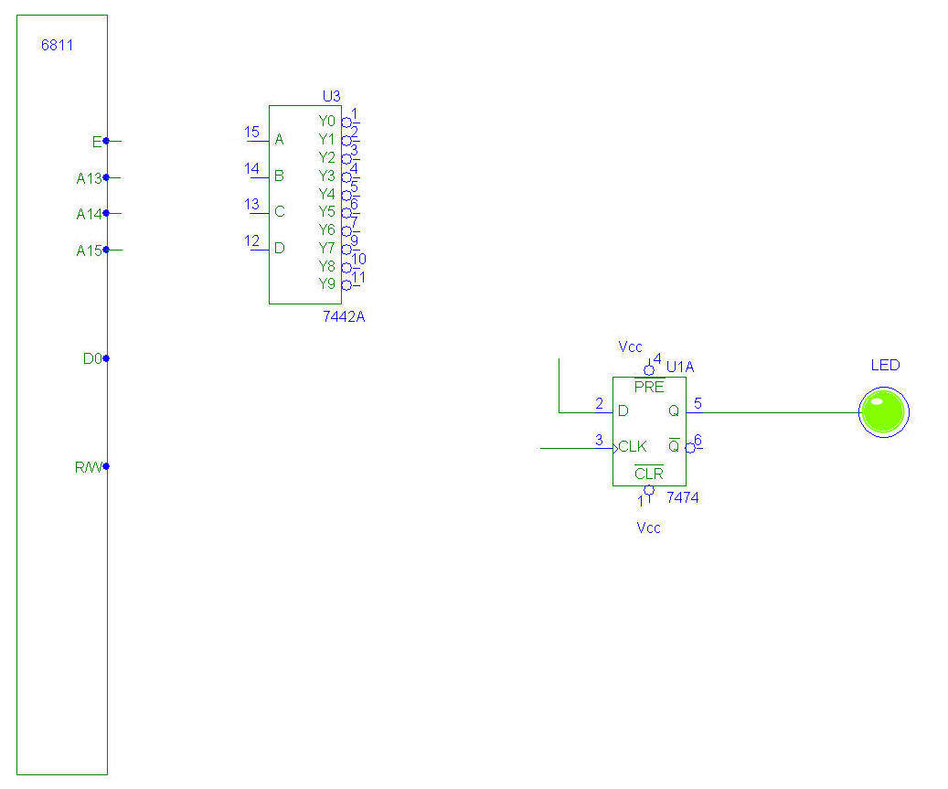
You may use the figure below to create your full design.
Handouts
Memory Address Map of the Heathkit
 <center>
