Difference between revisions of "CSC103 Logic Lab 2017"
(→Submission) |
|||
| Line 24: | Line 24: | ||
<bluebox> | <bluebox> | ||
| − | This lab is about logic design. Work in pairs and alternate with your lab partner when working at the keyboard. You do not have to turn in anything at the end of the lab. The goal of the lab is to get you to play with a logic gate simulator. | + | This lab is about logic design. Work in pairs and alternate with your lab partner when working at the keyboard. You do not have to turn in anything at the end of the lab. The goal of the lab is to get you to play with a logic gate simulator, and create a binary adder. |
</bluebox> | </bluebox> | ||
<br /> | <br /> | ||
<br /> | <br /> | ||
| + | <showafterdate after="20170920" before="20171231"> | ||
=Logic Simulator= | =Logic Simulator= | ||
| Line 318: | Line 319: | ||
<Br /> | <Br /> | ||
| − | + | </showafterdate> | |
<Br /> | <Br /> | ||
Revision as of 13:11, 19 September 2017
--D. Thiebaut (talk) 11:45, 19 September 2017 (EDT)
<meta name="keywords" content="computer science, How Computers Work, Dominique Thiebaut, smith college" /> <meta name="description" content="Dominique Thiebaut's Web Page" /> <meta name="title" content="Dominique Thiebaut -- Computer Science" /> <meta name="abstract" content="Dominique Thiebaut's Computer Science Web pages" /> <meta name="author" content="thiebaut at cs.smith.edu" /> <meta name="distribution" content="Global" /> <meta name="revisit-after" content="10 days" /> <meta name="copyright" content="(c) D. Thiebaut 2000, 2001, 2002, 2003, 2004, 2005, 2006, 2007,2008" /> <meta name="robots" content="FOLLOW,INDEX" />
Contents
This lab is about logic design. Work in pairs and alternate with your lab partner when working at the keyboard. You do not have to turn in anything at the end of the lab. The goal of the lab is to get you to play with a logic gate simulator, and create a binary adder.
<showafterdate after="20170920" before="20171231">
Logic Simulator
Reference
- We will be using LOGIC.LY's simulator for this lab. It's a superior simulator with a very natural interface.
- You can find a nice description of the simulator used in this lab at https://logic.ly/help/?utm_source=logicly-demo&utm_content=menu-help
The Simulator
- Go to logic.ly to start the simulator
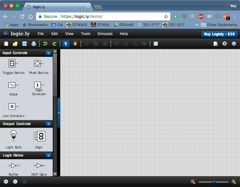
NOT, OR, and AND gates
Study all three fundamental gates: the NOT gate, the OR gate, and the AND gate.
The NOT gate
- Drag a Toggle Switch symbol from to the top-left section of the menu to the wiring area. Position it to the left. This will be your input.
- Drag a Light Bulb symbol on the rightmost part of the wiring area. Position it to the right. This will be your output.
- Drag a NOT gate from the Logic Gates area to the middle of the area.
- Connect the switch to the input of the NOT gate with a wire (left click and drag), and the output of the NOt gate to the light bulb with another wire.
- Click on the switch symbol to generate a 1 (blue color) or a zero (white). Try all possible variations of the input and verify that the output value is always the opposite of the input value.
Remember that you can drag symbols around to reposition them, if necessary.
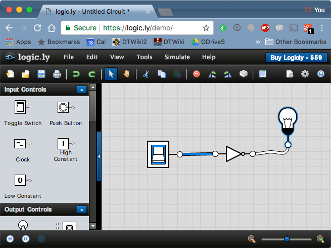
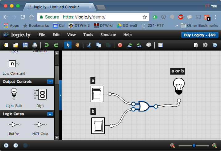
Once you're done, clear your wiring area and wire up an OR gate, as shown below:
The OR gate
- Take the similar steps as you did for the NOT gate, and wire up an OR gate with 2 inputs (you will be asked for the number of inputs when you drag the symbol to wiring area).
- Add a label (very bottom part of the left menu of symbols) above each of the two switches, and above the light bulb.
- Add wires between the switches and the inputs of the gate.
- Add a wire between the output of the gate and the light bulb.
- Try all possible combinations of the two inputs and verify that it's truth table is the following one:
| a | b | a OR b |
| 0 | 0 | 0 |
| 0 | 1 | 1 |
| 1 | 0 | 1 |
| 1 | 1 | 1 |
The AND gate
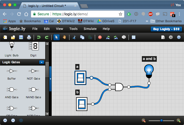
Take the similar steps as you did for the OR gate, and wire up an AND gate with 2 inputs. Try all possible combinations of the two inputs and verify that it's truth table is the following one:
| a | b | a AND b |
| 0 | 0 | 0 |
| 0 | 1 | 0 |
| 1 | 0 | 0 |
| 1 | 1 | 1 |
Binary Adder
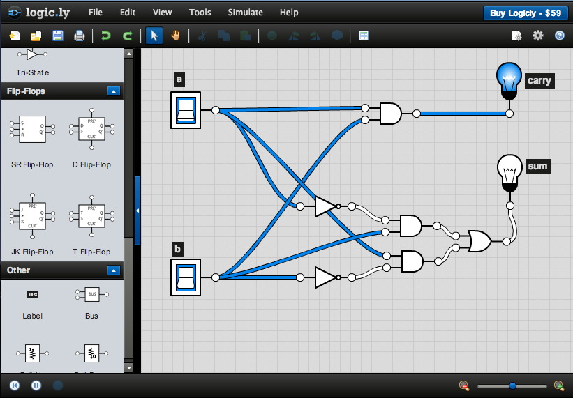
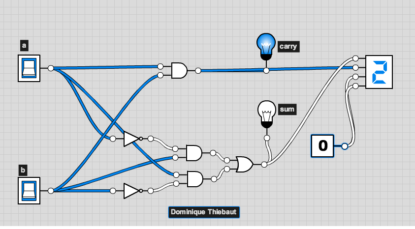
Wire up the circuit of the binary adder which we have seen in class.
Try all possible combinations of the inputs, and verify that the outputs correspond to the sum of the two inputs, in binary.
| a | + | b | = | carry | sum | |
|---|---|---|---|---|---|---|
| 0 | + | 0 | = | 0 | 0 | |
| 0 | + | 1 | = | 0 | 1 | |
| 1 | + | 0 | = | 0 | 1 | |
| 1 | + | 1 | = | 1 | 0 |
Playing with a Digit
- Do not erase your binary adder. Simply work in a different part of the wiring area.
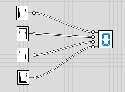
- Implement the circuit below:
- Activate the switches and try to make the digit show 0, then 1, then 2, etc. Stop at 9. Do not worry about the strange characters that may show up for some of the combinations of inputs.
Adding a Decimal Digit to the Adder
- We humans are not very good at understanding binary. Decimal is much more natural. This is why we have special circuits that take binary signals and display their decimal equivalent on LEDs that have the shape of decimal digits. The 7-segment display or Digit is such a device. You will find it next to the Light Bulb.
- Add a digit to your binary adder circuit, to the right of the two light bulbs.
- Connect the sum signal to the top input of the digit.
- Connect the carry signal to the next input of the digit.
- Set the other two inputs to 0, which you create with a Low Constant (see diagram below).
Submission
- When you are done with a design for the binary adder that works, add a text label in the lower part of the wiring areal, with your name (and that of your lab partner), as illustrated in the image below (I used my name for this example):
- Take a screen capture of your design (limit it to just the wiring area if possible) and submit that image to Moodle, in the Logic Design Lab section. If you do not know how to take a screen capture, see the last section of this lab for pointers.
3-Bit Adder (Optional)
- I am assuming that some of you will go through this lab very fast because you may have done some digital electronics before. For those only, you may want to sink your teeth into a tougher circuit, which is a 3-bit adder.
- A 3-bit adder is a circuit with 3 inputs, or bits, and two outputs, corresponding to the carry and the sum, similarly to the 2-bit adder.
- On a piece of paper, write the truth table for the 3-bit adder.
| b1 | b2 | b3 | carry | sum |
| 0 | 0 | 0 | ||
| 0 | 0 | 1 | ||
| 0 | 1 | 0 | ||
| 0 | 1 | 1 | ||
| 1 | 0 | 0 | ||
| 1 | 0 | 1 | ||
| 1 | 1 | 0 | ||
| 1 | 1 | 1 |
- Generate the boolean equations (using a, b, c, AND, OR and NOT) for the sum and the carry.
- Use the simulator to verify that the logic expression for the carry bit can also be realized by a different equation, very likely shorter than the one you found (there can be many equations that result in the same behavior):
carry = ( a AND b ) OR ( a AND c ) OR ( b AND c )
- Once you have wired and tested it, demonstrate it to your instructor! :-)
Hope you enjoyed the lab!
How to Take a Screen Capture
- With Windows: See https://www.digitalcitizen.life/4-ways-take-screenshots-windows-8-81-using-built-tools
- With Mac OS X: See https://support.apple.com/en-us/HT201361
</showafterdate>
