Difference between revisions of "CSC103 Exercise: Functional Description to Logic Design"
(→The Problem) |
(→The Problem) |
||
| (One intermediate revision by the same user not shown) | |||
| Line 10: | Line 10: | ||
=The Problem= | =The Problem= | ||
| − | + | Create a circuit made of AND, OR, and NOT gates that computes the majority of three bits. | |
| − | |||
| − | |||
<br /> | <br /> | ||
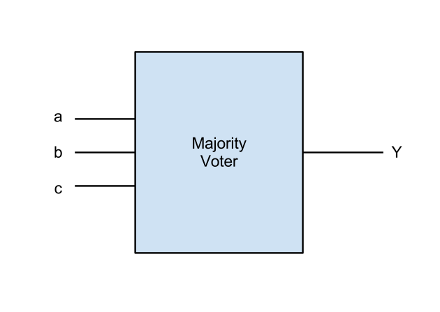
| − | + | <center>[[Image:majorityVoterBlank.png|300px]]</center> | |
<br /> | <br /> | ||
| + | |||
;Question 1 | ;Question 1 | ||
| − | : Generate the truth table | + | : Generate the truth table for this circuit |
| + | |||
| + | ;Question 2 | ||
| + | : Generate the boolean expression for the output signal | ||
| + | |||
| + | ;Question 3 | ||
| + | : Translate the equation into a logic circuit with AND, OR, and NOT gates | ||
| + | |||
| + | ;Question 4 | ||
| + | : How could you verify that your circuit is accurate? | ||
<br /> | <br /> | ||
Latest revision as of 08:32, 8 February 2012
--D. Thiebaut 22:12, 7 February 2012 (EST)
This exercise illustrates the process of going from the formulation of a problem to the design of a solution that involves AND, OR and NOT logic circuits.
The Problem
Create a circuit made of AND, OR, and NOT gates that computes the majority of three bits.

- Question 1
- Generate the truth table for this circuit
- Question 2
- Generate the boolean expression for the output signal
- Question 3
- Translate the equation into a logic circuit with AND, OR, and NOT gates
- Question 4
- How could you verify that your circuit is accurate?