Difference between revisions of "CSC270 Homework 9 2012"
(→Problem #2) |
(→Problem #3) |
||
| (5 intermediate revisions by the same user not shown) | |||
| Line 2: | Line 2: | ||
---- | ---- | ||
<bluebox> | <bluebox> | ||
| − | This assignment is due on 4/18/12, at the beginning of the lab. | + | This assignment is due on 4/18/12, at the beginning of the lab. You can work on this homework in groups of at most 2 people. |
</bluebox> | </bluebox> | ||
| Line 19: | Line 19: | ||
=Problem #2= | =Problem #2= | ||
| − | Same question with the hardware shown below. Y1' from the 7442 is connected to the CLR' input of the 7474. Y3' of the 7442 is connected to the PR' input of the 7474. Both the D and clock inputs of the 7474 are grounded. | + | Same question with the hardware shown below. This time the wiring is even more interesting... Y1' from the 7442 is connected to the CLR' input of the 7474. Y3' of the 7442 is connected to the PR' input of the 7474. Both the D and clock inputs of the 7474 are grounded. |
Write the driver (2 functions) that can be used to turn the LED either ON, or OFF. | Write the driver (2 functions) that can be used to turn the LED either ON, or OFF. | ||
| Line 29: | Line 29: | ||
=Problem #3= | =Problem #3= | ||
| − | + | For this problem you have to design the hardware and write the software for a new port that will interface with the 6811. The hardware interface should activate an LED that will either blink at 500 KHz, or not blink at all, in which case it will stay OFF. | |
You need to propose a design that combines both hardware and software. | You need to propose a design that combines both hardware and software. | ||
| − | + | You should present your hardware design in the form of a schematic diagram (see above for inspiration). | |
| − | The software design should be just two functions, one to activate the 500 KHz oscillation. The other turn the oscillation OFF. For example, | + | The software design should be just two functions, one to activate the 500 KHz oscillation. The other to turn the oscillation OFF. For example, below is a simple program that uses the two functions you have to write. The documentation explains what is going on. |
<source lang="asm"> | <source lang="asm"> | ||
| Line 46: | Line 46: | ||
jmp start | jmp start | ||
| + | oscillate: | ||
| + | ... ;your code goes here | ||
| + | rts | ||
| + | |||
| + | turnLEDOff: | ||
| + | ... ;your code goes here | ||
| + | rts | ||
</source> | </source> | ||
<br /><br /><br /><br /><br /><br /><br /><br /><br /><br /><br /><br /><br /> | <br /><br /><br /><br /><br /><br /><br /><br /><br /><br /><br /><br /><br /> | ||
[[Category:CSC270]][[Category:Homework]][[Category:6811]] | [[Category:CSC270]][[Category:Homework]][[Category:6811]] | ||
Latest revision as of 06:52, 12 April 2012
--D. Thiebaut 15:31, 11 April 2012 (EDT)
This assignment is due on 4/18/12, at the beginning of the lab. You can work on this homework in groups of at most 2 people.
Problem #1
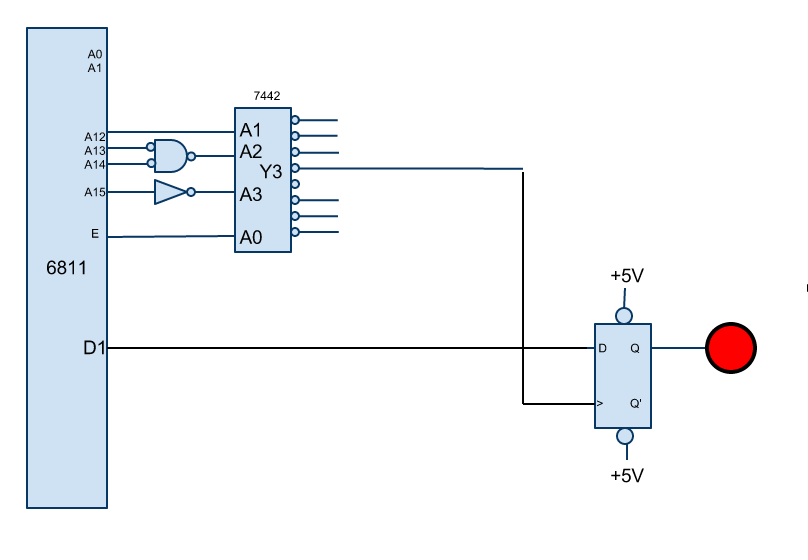
Write the driver for the hardware shown below, that consists of a 1-bit port attached to a red LED. The driver should be a collection of 2 functions, one to turn the LED ON, and another function to turn the LED OFF.
Note that who ever designed this circuit didn't use the same approach you took in the lab. In particular this design is more expensive in terms of gates. Also, make sure you notice that the port is connected to D1 of the Data Bus, and not D0 as you did in the lab...
Problem #2
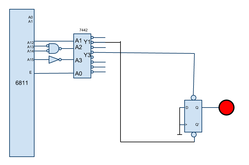
Same question with the hardware shown below. This time the wiring is even more interesting... Y1' from the 7442 is connected to the CLR' input of the 7474. Y3' of the 7442 is connected to the PR' input of the 7474. Both the D and clock inputs of the 7474 are grounded.
Write the driver (2 functions) that can be used to turn the LED either ON, or OFF.
Problem #3
For this problem you have to design the hardware and write the software for a new port that will interface with the 6811. The hardware interface should activate an LED that will either blink at 500 KHz, or not blink at all, in which case it will stay OFF.
You need to propose a design that combines both hardware and software.
You should present your hardware design in the form of a schematic diagram (see above for inspiration).
The software design should be just two functions, one to activate the 500 KHz oscillation. The other to turn the oscillation OFF. For example, below is a simple program that uses the two functions you have to write. The documentation explains what is going on.
	org	0000
start:  jsr	oscillate	;make hardware start 500KHz oscillation
        jsr	C027		;make oscillations last 1 second
        jsr	turnLEDOff	;stop oscillations
        jsr	C027		;LED stays off for 2 seconds
        jsr	C027
        jmp	start

oscillate:
        ...                     ;your code goes here
        rts

turnLEDOff:
        ...                     ;your code goes here
        rts

