Difference between revisions of "CSC231 Logic Design Lab 2014"
(Created page with "--~~~~ ---- __TOC__ <br /> <br /> <center> =Logic Design LAB= </center> ==Data Sheets== If you need to refer to the data sheets of various chips during the lab, you can...") |
(→Useful Boolean Axioms) |
||
| (30 intermediate revisions by the same user not shown) | |||
| Line 9: | Line 9: | ||
=Logic Design LAB= | =Logic Design LAB= | ||
</center> | </center> | ||
| − | + | <bluebox> | |
| + | This lab is worth 100 points. You get the 100 points when you demonstrate that you can add 2 bits and get a correct sum and carry. You do not need to provide a lab report for this lab. | ||
| + | </bluebox> | ||
| − | == | + | ==EXPERIMENT #1: INVESTIGATING THE KIT== |
| − | + | <br /> | |
| − | + | ===Overview of the Kit=== | |
| − | + | <br /> | |
| − | [ | + | <center>[[Image:DigitalKit.jpg|550px]]</center> |
| − | + | <br /> | |
| − | + | The main tools for us today are the switches, the LEDs, the +5 and GND wiring plots, and the ''breadboard'' area. You will put ''Integrated Circuits'' (ICs) on the breadboard area. | |
| + | <br /> | ||
| − | == | + | ===Exploration=== |
| − | + | <br /> | |
| − | For this part, concentrate only on the flatter part of the Digital Kit, not the circuit board that is upright, facing you. Please follow the steps below. | + | For this part, concentrate only on the '''flatter''' part of the Digital Kit, not the ''vertical'' circuit board that is upright, facing you. Please follow the steps below. |
# '''Power OFF'''. <font color="red">Always turn OFF the power when you are wiring circuits. This will prevent shorts and extend the life of your circuits.</font> | # '''Power OFF'''. <font color="red">Always turn OFF the power when you are wiring circuits. This will prevent shorts and extend the life of your circuits.</font> | ||
# Connect a wire between the Logic Indicator '''L4''' and the '''Logic Switch A'''. | # Connect a wire between the Logic Indicator '''L4''' and the '''Logic Switch A'''. | ||
| Line 27: | Line 30: | ||
# Activate Switch A, and observe the LED (Light Emitting Diode) turn ON and OFF. | # Activate Switch A, and observe the LED (Light Emitting Diode) turn ON and OFF. | ||
# '''Power OFF''' | # '''Power OFF''' | ||
| − | # Switch the wire from A to A-Bar, turn the power back ON, and see how the LED reacts . | + | # Switch the wire from A to A-Bar, turn the power back ON, and see how the LED reacts .<br /><br /><br /> |
| − | <br /> | + | # Same experiment, but this time replace the Logic Switch by one of the '''Data Switches'''.<br /><br /><br /> |
| − | # Same experiment, but this time replace the Logic Switch by one of the '''Data Switches'''. | ||
| − | <br /> | ||
# '''Power OFF'''. | # '''Power OFF'''. | ||
# Connect one of the Logic Indicators to the Clock signal. Connect a second wire from another Logic Indicator to the Clock-bar signal. Make sure the sliding switch is on the 1Hz mark. | # Connect one of the Logic Indicators to the Clock signal. Connect a second wire from another Logic Indicator to the Clock-bar signal. Make sure the sliding switch is on the 1Hz mark. | ||
| Line 39: | Line 40: | ||
==EXPERIMENT #2: INTEGRATED CIRCUITS AND LOGIC GATES== | ==EXPERIMENT #2: INTEGRATED CIRCUITS AND LOGIC GATES== | ||
| + | <br /> | ||
| + | Below are the simplified data sheets for the Integrated Circuits you will use today. | ||
| + | {| | ||
| + | | | ||
| + | [[Image:7404.png]] | ||
| + | | | ||
| + | Inverter: 74LS04 | ||
| + | |- | ||
| + | | | ||
| + | [[Image:7408.png]] | ||
| + | | | ||
| + | AND gate: 74LS08 | ||
| + | |- | ||
| + | | | ||
| + | [[Image:7432.png]] | ||
| + | | | ||
| + | OR gate: 74LS32 | ||
| + | |- | ||
| + | | | ||
| + | [[Image:7486.png]] | ||
| + | | | ||
| + | Exclusive OR: 74LS86 | ||
| + | |} | ||
| + | <br /> | ||
| − | + | '''Note:''' The XOR is not a ''universal'' gate, but its function is encountered enough times in the real world that manufacturers have built a circuit just for this function. The equation for ''a XOR b'' is ''( a and not b ) or ( not a and b)'', which can be implemented using the simple AND, OR, and NOT. | |
| − | + | <br /> | |
| − | + | ===Testing === | |
| − | |||
| − | |||
| − | |||
| − | |||
| − | |||
| − | |||
| − | |||
| + | * <font color="Red">Power OFF</font> | ||
| + | * Put a 74LS08 on the breadboard. | ||
| + | <br /> | ||
| + | <blockquote> | ||
<tanbox> | <tanbox> | ||
;Rule 1 | ;Rule 1 | ||
:Always make sure the notch on the circuit is facing left. This way the circuit matches the diagram on the datasheets. | :Always make sure the notch on the circuit is facing left. This way the circuit matches the diagram on the datasheets. | ||
</tanbox> | </tanbox> | ||
| + | </blockquote> | ||
<br /> | <br /> | ||
| + | * Connect its pin 14 to +5V. See Figure 1 below for illustration of this step. | ||
| + | * Connect its pin 7 to GND. | ||
| + | <blockquote> | ||
<tanbox> | <tanbox> | ||
;Rule 2 | ;Rule 2 | ||
: Always make sure that the circuit is connected to +5V through its pin 14, and to GND via its pin 7. | : Always make sure that the circuit is connected to +5V through its pin 14, and to GND via its pin 7. | ||
</tanbox> | </tanbox> | ||
| − | + | </blockquote> | |
| + | * Connect Pin 1 to a data switch. | ||
| + | * Connect the Data Switch you just used to one of the Logic Indicators. | ||
| + | * Connect Pin 2 to a data switch. | ||
| + | * Connect the Data Switch you just used to another the Logic Indicators. | ||
| + | * Connect Pin 3 to a third Logic Indicator. | ||
| + | * <font color="Red">Power ON</font> | ||
| + | * Activate the different data switches. | ||
| + | * Verify that your circuit implements an AND boolean operator. | ||
| + | <br /> | ||
| + | * Leave the wires as they are, and remove the 74LS08 being careful not to disconnect any of the wires. | ||
| + | * Replace the 74LS08 by the 74LS86. | ||
| + | * Verify that the new circuit implements an XOR operator. | ||
| + | <br /> | ||
| + | * Leave the wires as they are, and remove the 74LS86 being careful not to disconnect any of the wires. | ||
| + | * Replace the 74LS86 by the 74LS32. | ||
| + | * Verify that the new circuit implements an OR operator. | ||
| + | <br /> | ||
| + | * We'll skip the 74LS04, since this circuit is not pin-to-pin compatible with the other 3 (look at the schematic above to verify that this is, indeed, not the case). | ||
| Line 69: | Line 113: | ||
'''Figure 1''':''Wiring of an IC on the breadboard. Always identify pin 1 of the IC which is on the left (or below) the notch or circle embossed on the top of the chip'' | '''Figure 1''':''Wiring of an IC on the breadboard. Always identify pin 1 of the IC which is on the left (or below) the notch or circle embossed on the top of the chip'' | ||
| − | + | <br /> | |
| − | + | =2-Bit Adder= | |
| − | + | <br /> | |
| − | + | <blockquote> | |
| − | + | <bluebox> | |
| − | + | If you are ambitious and feel you have at least 30 minutes left ahead of you, select to implement the 2-bit adder with only AND, OR, and NOT operators. If you are interested in a simpler solution with fewer wires, implement the 2-bit adder with an AND and an XOR operator. | |
| − | + | </bluebox> | |
| − | + | </blockquote> | |
| − | + | <br /> | |
| − | + | * Generate the equations for the Carry and Sum bits as the sum of two bits B1 and B2. | |
| − | + | * Wire up the circuit. | |
| − | -- | ||
| − | |||
| − | |||
| − | |||
| − | |||
| − | |||
| − | |||
| − | |||
| − | |||
| − | |||
| − | |||
| − | |||
| − | |||
| − | |||
| − | |||
| − | |||
| − | |||
| − | |||
| + | <br /> | ||
| + | <br /> | ||
| + | =3-Bit Adder= | ||
| + | <br /> | ||
| + | * If you are ''really'' ambitious and have time, implement a 3-bit adder! | ||
| + | <br /> | ||
| + | <center>[[Image:CSC270BreadboardArea.png]]</center> | ||
| + | <br /> | ||
| + | <br /> | ||
| − | + | ||
| − | |||
| − | |||
| − | |||
| − | |||
| − | |||
| − | |||
| − | |||
| − | |||
| − | |||
| − | |||
| − | |||
| − | |||
| − | |||
| − | |||
| − | |||
| − | |||
| − | |||
| − | |||
| − | |||
| − | |||
| − | |||
| − | |||
| − | |||
| − | |||
| − | |||
| − | |||
| − | |||
| − | |||
| − | |||
| − | |||
| − | |||
| − | |||
| − | |||
| − | |||
| − | |||
| − | |||
| − | |||
| − | |||
| − | |||
| − | |||
| − | |||
| − | |||
| − | |||
| − | |||
| − | |||
| − | |||
| − | |||
| − | |||
| − | |||
| − | |||
| − | |||
| − | |||
| − | |||
| − | |||
| − | |||
| − | == | + | ==Useful Boolean Axioms== |
| − | + | <br /> | |
| − | + | * You may find these axioms useful in simplifying functions (taken from [http://en.wikipedia.org/wiki/Boolean_algebra_(structure) Wikipedia]) | |
| − | |||
| − | |||
| − | |||
| − | |||
| − | |||
| − | |||
| − | |||
| − | |||
| − | |||
| − | |||
| − | |||
| − | |||
| − | |||
| − | |||
| − | |||
| − | |||
| − | |||
| − | |||
| − | |||
| − | |||
| − | |||
| − | |||
| − | |||
| − | |||
| − | |||
| − | |||
| − | |||
| − | |||
| − | |||
| − | |||
| − | |||
| − | |||
| − | |||
| − | |||
| − | |||
| − | |||
| − | |||
::{| cellpadding=5 | ::{| cellpadding=5 | ||
| Line 222: | Line 165: | ||
|} | |} | ||
| − | + | ||
| − | |||
| − | |||
| − | |||
| − | |||
| − | |||
| − | |||
| − | |||
| − | |||
| − | |||
| − | |||
| − | |||
| − | |||
| − | |||
| − | |||
| − | |||
| − | |||
| − | |||
| − | |||
| − | |||
| − | |||
| − | |||
| − | |||
| − | |||
| − | |||
| − | |||
| − | |||
| − | |||
| − | |||
| − | |||
| − | |||
| − | |||
| − | |||
| − | |||
| − | |||
| − | |||
| − | |||
| − | |||
| − | |||
| − | |||
| − | |||
| − | |||
| − | |||
<br /> | <br /> | ||
| Line 276: | Line 177: | ||
<br /> | <br /> | ||
| − | [[Category: | + | [[Category:CSC231]][[Category:Labs]] |
Latest revision as of 13:30, 19 November 2014
--D. Thiebaut (talk) 10:35, 19 November 2014 (EST)
Contents
Logic Design LAB
This lab is worth 100 points. You get the 100 points when you demonstrate that you can add 2 bits and get a correct sum and carry. You do not need to provide a lab report for this lab.
EXPERIMENT #1: INVESTIGATING THE KIT
Overview of the Kit
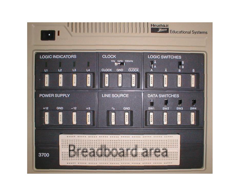
The main tools for us today are the switches, the LEDs, the +5 and GND wiring plots, and the breadboard area. You will put Integrated Circuits (ICs) on the breadboard area.
Exploration
For this part, concentrate only on the flatter part of the Digital Kit, not the vertical circuit board that is upright, facing you. Please follow the steps below.
- Power OFF. Always turn OFF the power when you are wiring circuits. This will prevent shorts and extend the life of your circuits.
- Connect a wire between the Logic Indicator L4 and the Logic Switch A.
- Power ON
- Activate Switch A, and observe the LED (Light Emitting Diode) turn ON and OFF.
- Power OFF
- Switch the wire from A to A-Bar, turn the power back ON, and see how the LED reacts .
- Same experiment, but this time replace the Logic Switch by one of the Data Switches.
- Power OFF.
- Connect one of the Logic Indicators to the Clock signal. Connect a second wire from another Logic Indicator to the Clock-bar signal. Make sure the sliding switch is on the 1Hz mark.
- Power UP. What do you observe?
- Slide the switch to 1KHz. What happens? Why? Is there any difference in the brightness of the LED? Why?
EXPERIMENT #2: INTEGRATED CIRCUITS AND LOGIC GATES
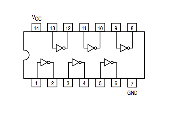
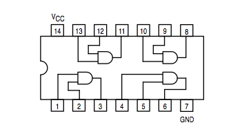
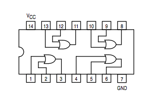
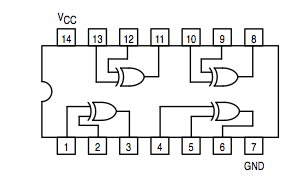
Below are the simplified data sheets for the Integrated Circuits you will use today.
|
Inverter: 74LS04 | |
|
AND gate: 74LS08 | |
|
OR gate: 74LS32 | |
|
Exclusive OR: 74LS86 |
Note: The XOR is not a universal gate, but its function is encountered enough times in the real world that manufacturers have built a circuit just for this function. The equation for a XOR b is ( a and not b ) or ( not a and b), which can be implemented using the simple AND, OR, and NOT.
Testing
- Power OFF
- Put a 74LS08 on the breadboard.
- Rule 1
- Always make sure the notch on the circuit is facing left. This way the circuit matches the diagram on the datasheets.
- Connect its pin 14 to +5V. See Figure 1 below for illustration of this step.
- Connect its pin 7 to GND.
- Rule 2
- Always make sure that the circuit is connected to +5V through its pin 14, and to GND via its pin 7.
- Connect Pin 1 to a data switch.
- Connect the Data Switch you just used to one of the Logic Indicators.
- Connect Pin 2 to a data switch.
- Connect the Data Switch you just used to another the Logic Indicators.
- Connect Pin 3 to a third Logic Indicator.
- Power ON
- Activate the different data switches.
- Verify that your circuit implements an AND boolean operator.
- Leave the wires as they are, and remove the 74LS08 being careful not to disconnect any of the wires.
- Replace the 74LS08 by the 74LS86.
- Verify that the new circuit implements an XOR operator.
- Leave the wires as they are, and remove the 74LS86 being careful not to disconnect any of the wires.
- Replace the 74LS86 by the 74LS32.
- Verify that the new circuit implements an OR operator.
- We'll skip the 74LS04, since this circuit is not pin-to-pin compatible with the other 3 (look at the schematic above to verify that this is, indeed, not the case).
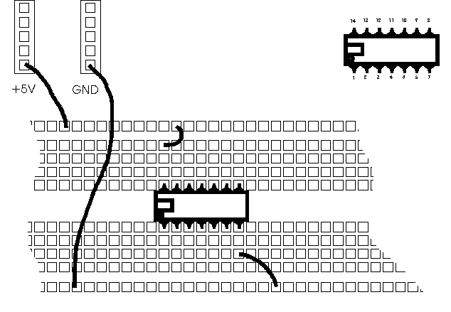
Figure 1:Wiring of an IC on the breadboard. Always identify pin 1 of the IC which is on the left (or below) the notch or circle embossed on the top of the chip
2-Bit Adder
If you are ambitious and feel you have at least 30 minutes left ahead of you, select to implement the 2-bit adder with only AND, OR, and NOT operators. If you are interested in a simpler solution with fewer wires, implement the 2-bit adder with an AND and an XOR operator.
- Generate the equations for the Carry and Sum bits as the sum of two bits B1 and B2.
- Wire up the circuit.
3-Bit Adder
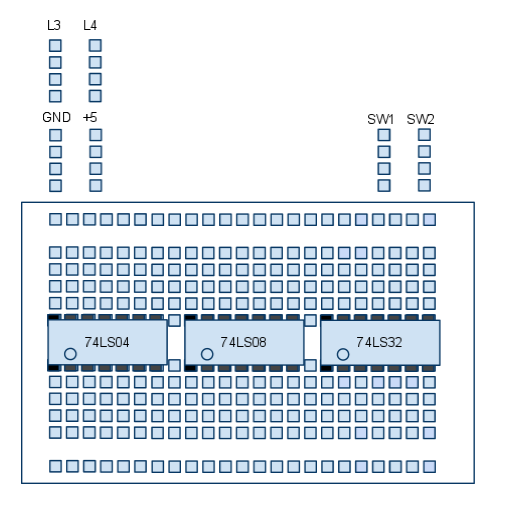
- If you are really ambitious and have time, implement a 3-bit adder!
Useful Boolean Axioms
- You may find these axioms useful in simplifying functions (taken from Wikipedia)
a OR (b OR c) = (a OR b) OR c a AND (b AND c) = (a AND b) AND c Associativity a OR b = b OR a a AND b = b AND a Commutativity a OR (a AND b) = a a AND (a OR b) = a Absorption a OR (b AND c) = (a OR b) AND (a OR c) a AND (b OR c) = (a AND b) OR (a AND c) Distributivity a OR NOT a = 1 a AND NOT a = 0 Complements
