Difference between revisions of "CSC270 Lab 2 2016"
(→The 74LS42 Datasheet) |
(→Experiment #1) |
||
| (2 intermediate revisions by the same user not shown) | |||
| Line 81: | Line 81: | ||
<br /> | <br /> | ||
The 74LS42 is an ''integrated'' decoder. Decoders are so common in computers, that putting one in a chip made sense for the chip manufacturers. | The 74LS42 is an ''integrated'' decoder. Decoders are so common in computers, that putting one in a chip made sense for the chip manufacturers. | ||
| + | <br /> | ||
| + | <tanbox>Be careful, this circuit has 16 pins, and not 14, as we have been using so far!</tanbox> | ||
| + | <br /> | ||
<center> | <center> | ||
[[Image:74ls42a.png|400px]] | [[Image:74ls42a.png|400px]] | ||
| Line 100: | Line 103: | ||
:Are the outputs active high or active low? | :Are the outputs active high or active low? | ||
| − | Using the schematics as your guide, design a 2-bit adder using this decoder, and as few other integrated circuits as possible. The fewer chips on your breadboard the better! | + | ;Question 3: |
| + | :Using the schematics as your guide, design a 2-bit adder using this decoder, and as few other integrated circuits as possible. The fewer chips on your breadboard the better! | ||
<br /> | <br /> | ||
| − | |||
| − | |||
| − | |||
| − | |||
| − | |||
| − | |||
| − | |||
<br /> | <br /> | ||
| Line 119: | Line 116: | ||
<br /> | <br /> | ||
<br /> | <br /> | ||
| + | [[Category:CSC270]][[Category:Labs]] | ||
Latest revision as of 20:47, 3 February 2016
--D. Thiebaut (talk) 20:15, 3 February 2016 (EST)
Contents
Nand Gates
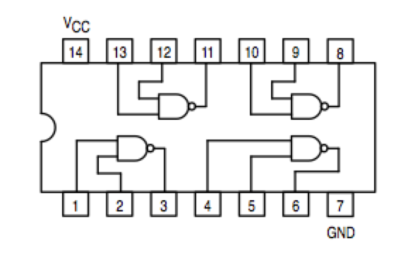
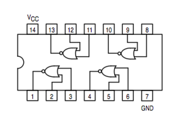
- Implement the 2-bit adder with NAND gates only. The figures below show the schematics of a NAND gate (and of a NOR gate, for completeness).
|
|
Hints: You may use the A, A', B, and B' logic switches if that can help you simplify your circuit. Less is more!
Decoder Circuit: the Do-It-Yourself version
Part 1
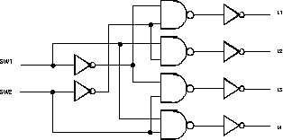
Complete the circuit shown in Figure 1 by adding the part numbers of the circuits. Add this number inside the logic symbol, and also add the pin numbers on the inputs and outputs of the gates. Also, do not forget that each circuit requires power and ground.
- When you are done, implement the circuit on the breadboard section of your kit.
- Make sure you have turned off the power before you start wiring.
- Also, make sure that you connect the outputs of the inverters to the four logic indicators (LEDs). Verify your connections before you turn the power back on. Activate the two inputs and record the outputs in a truth table which you'll include in your report.
 SW1 	SW2 	L4 	L3 	L2 	L1
 0 	0
 0 	1
 1 	0
 1 	1
Because the inactive outputs are all set to zero, and the active one is set to 1, we refer to this type of circuit as a circuit with "active high" outputs.
Part 2
Now connect L1, L2, L3 and L4 to the input of the inverters rather than their output, and record the variation of L4, L3, L2 and L1 as a function of SW2 and SW1.
 SW1 	SW2 	L4 	L3 	L2 	L1
 0 	0
 0 	1
 1 	0
 1 	1
You now have the opposite behavior, where the inactive outputs are all 1 except for one that is set to 0. We refer to this type of circuit as a circuit with active-low outputs.
Most decoders work as the last circuit you just tested, rather than the one you first experimented with, although the first circuit had a more "intuitive" behavior.
The 74LS42 Datasheet
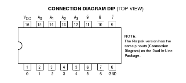
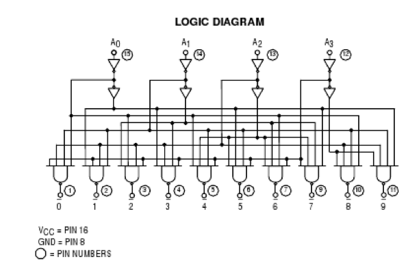
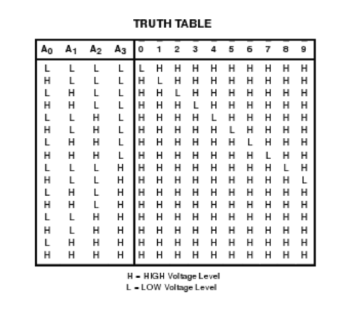
The 74LS42 is an integrated decoder. Decoders are so common in computers, that putting one in a chip made sense for the chip manufacturers.
Experiment #1
Study the 74LS42 data-sheet. Observe it carefully and figure out what kind of decoder it is:
- Question 1
- Is it a 3-to-8 decoder? A 4-to-16 decoder? If not, then what?
- Question 2
- Are the outputs active high or active low?
- Question 3
- Using the schematics as your guide, design a 2-bit adder using this decoder, and as few other integrated circuits as possible. The fewer chips on your breadboard the better!
