Difference between revisions of "CSC270 Lab 7"
(→Step 2: R/W') |
(→Capturing Irregular Waveforms) |
||
| (10 intermediate revisions by the same user not shown) | |||
| Line 1: | Line 1: | ||
| − | = | + | =Part I: the Oscilloscope= |
<center>[[Image:CSC270_Oscilloscope.jpg]]</center> | <center>[[Image:CSC270_Oscilloscope.jpg]]</center> | ||
| Line 116: | Line 116: | ||
* Play with the ''holdoff'' button and increase the delay to about 15 ~ 17 µs until you get a stable waveform, similar to that shown below: | * Play with the ''holdoff'' button and increase the delay to about 15 ~ 17 µs until you get a stable waveform, similar to that shown below: | ||
| − | <center>[[Image:CSC270_scopeWaveform2.jpg | | + | <center>[[Image:CSC270_scopeWaveform2.jpg | 500px ]]</center> |
| Line 191: | Line 191: | ||
* How often does your loop repeat in one second (here again make the scope give you the answer)? _____________ | * How often does your loop repeat in one second (here again make the scope give you the answer)? _____________ | ||
| + | <!-- | ||
==Step 3: Benchmark programs and MIPS ratings== | ==Step 3: Benchmark programs and MIPS ratings== | ||
| Line 201: | Line 202: | ||
A way to quickly verify your answer is to measure the frequency of the LIR signal, which stands for Load Instruction Register, and which is activated high every time the processor loads an instruction op-code in the control unit. Think of it as a signal showing us the Instruction Fetch cycle of the 6811. Put a probe on LIR and ask the scope to give you its frequency. That's your MIPS rating! | A way to quickly verify your answer is to measure the frequency of the LIR signal, which stands for Load Instruction Register, and which is activated high every time the processor loads an instruction op-code in the control unit. Think of it as a signal showing us the Instruction Fetch cycle of the 6811. Put a probe on LIR and ask the scope to give you its frequency. That's your MIPS rating! | ||
| + | --> | ||
| − | == Step | + | == Step 3: Address Bits== |
The next step is to observe the behavior of the address bus during the loop. There are 16 bits of addresses, but since your program fits in only a few bytes of memory, most of the memory address bits remain the same during the program. Only the least significant bits change. For this reason we can simplify our task by monitoring the one that changes most: A0. A0 is the least significant bit, and will be 0 when the processor accesses an even address, and 1 otherwise. | The next step is to observe the behavior of the address bus during the loop. There are 16 bits of addresses, but since your program fits in only a few bytes of memory, most of the memory address bits remain the same during the program. Only the least significant bits change. For this reason we can simplify our task by monitoring the one that changes most: A0. A0 is the least significant bit, and will be 0 when the processor accesses an even address, and 1 otherwise. | ||
| Line 209: | Line 211: | ||
* Record the behavior of A0 on the timing diagram below, along with the other signal displayed (use two diagrams if your loop lasts longer than 10 cycles.) | * Record the behavior of A0 on the timing diagram below, along with the other signal displayed (use two diagrams if your loop lasts longer than 10 cycles.) | ||
| + | <br><br> | ||
| + | [[Image:CSC270_ScopeWindow.gif|350px]][[Image:CSC270_ScopeWindow.gif|350px]] | ||
| + | <br><br> | ||
| − | == Step | + | == Step 4: Data Bits== |
We will use the same technique to record the behavior of the data bus: we'll only observe D0. Remove the probe from A0 and connect it to D0 and record the behavior of the two waveforms. You will notice that D0 might look very strange compared to other signals... It is in part because it is generated sometimes by the processor, sometimes by the memory, and sometimes neither the processor nor memory is using the data-bus, and the signal is somehow allowed to "float"... | We will use the same technique to record the behavior of the data bus: we'll only observe D0. Remove the probe from A0 and connect it to D0 and record the behavior of the two waveforms. You will notice that D0 might look very strange compared to other signals... It is in part because it is generated sometimes by the processor, sometimes by the memory, and sometimes neither the processor nor memory is using the data-bus, and the signal is somehow allowed to "float"... | ||
| − | * Question: Why does D0 seem to be both high and low during the short time that R/W' is low, and that it seems impossible to synchronize the scope so as to show D0 in a stable form? Does this happen in other parts of the waveform as well? | + | * Question: Why does D0 seem to be both high and low during the short time that R/W' is low, and that it seems impossible to synchronize the scope so as to show D0 in a stable form? Does this happen in other parts of the waveform as well? |
== Putting it all together== | == Putting it all together== | ||
| − | Once the timing diagram is complete, isolate the cycles corresponding to individual instructions, and reconstruct the execution of the instructions | + | Once the timing diagram is complete, isolate the cycles corresponding to individual instructions, and reconstruct the execution of the instructions in a new timing diagram. Indicate in each cycle what is happening with the processor-memory system, as we have done in class this week. |
Use the information on the 6811 instructions at the end of this lab to figure out what the processor does during the execution of the instructions. If you are using an instruction that is not in the handout for this lab, simply go to the appendix of the 6811 manual and print the pages you need on your own. | Use the information on the 6811 instructions at the end of this lab to figure out what the processor does during the execution of the instructions. If you are using an instruction that is not in the handout for this lab, simply go to the appendix of the 6811 manual and print the pages you need on your own. | ||
| Line 224: | Line 229: | ||
Make sure you clearly highlight the cycles belonging to the different instructions of your program, and write at the bottom of each column what happens during the cycle (e.g. "op code fetch", "1st byte operand fetch", "internal cycle", etc.). Explain why the A0 or D0 bit is high or low during each cycle. | Make sure you clearly highlight the cycles belonging to the different instructions of your program, and write at the bottom of each column what happens during the cycle (e.g. "op code fetch", "1st byte operand fetch", "internal cycle", etc.). Explain why the A0 or D0 bit is high or low during each cycle. | ||
| − | + | <br><br> | |
| − | + | [[Image:CSC270_ScopeWindow.gif|350px]][[Image:CSC270_ScopeWindow.gif|350px]] | |
| − | + | <br><br> | |
| − | |||
| − | |||
| − | |||
| − | |||
| − | |||
| − | |||
| − | |||
| − | |||
| − | |||
| − | |||
| − | |||
| − | |||
| − | |||
| − | |||
| − | |||
| − | |||
| − | |||
| − | |||
| − | |||
| − | |||
| − | |||
| − | |||
| − | |||
| − | |||
| − | |||
| − | |||
| − | |||
| − | |||
| − | |||
| − | |||
| − | |||
| − | |||
| − | |||
| − | |||
| − | |||
| − | |||
| − | |||
| − | |||
| − | |||
| − | |||
| − | |||
| − | |||
| − | |||
| − | |||
| − | |||
| − | |||
| − | |||
| − | |||
| − | |||
| − | |||
| − | |||
| − | |||
| − | |||
| − | |||
| − | |||
| − | |||
| − | |||
| − | |||
| − | |||
| − | |||
| − | |||
| − | |||
| − | |||
| − | |||
| − | |||
| − | |||
| − | |||
| − | |||
| − | + | =Appendix: Instruction Timing= | |
| − | |||
| − | + | [[Image:CSC270_LDAA.png]] | |
| − | + | [[Image:CSC270_STAA.png]] | |
| − | + | [[Image:CSC270_JMP.png]] | |
| − | + | [[Image:CSC270_INC.png]] | |
Latest revision as of 11:38, 1 April 2009
Contents
Part I: the Oscilloscope
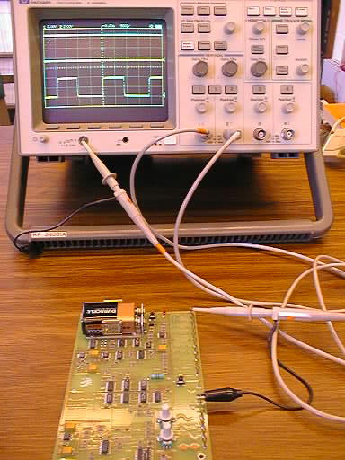
This section will follow a mini lecture on the oscilloscope and its typical features. We will go through each section below in synch, with black-board presentation and experiments interleaved.
Studying the calibration waveform
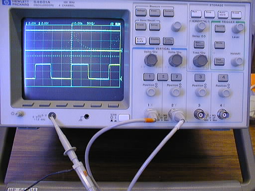
- Connect Probe 1 to the calibration test-point, as shown in the picture below:
- Press AutoScale
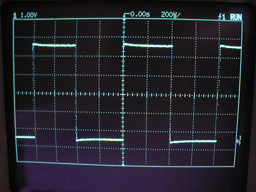
- Observe the waveform. It should look like this picture:
Moving the waveform on the screen.
To move it horizontally, find the Horizontal section on the front panel, and the Delay button. Turn it and observe how the waveform can be translated horizontally.
To move it vertically, find the Vertical section, and turn the Position knob in the Probe 1 column. See how you an move the waveform up and down.
Changing the scale of the waveform.
To change its horizontal scale, locate the Time/Div knob in the the Horizontal section. Play with it and see how you can "zoom" in and out, closer or farther away from the waveform.
To change the vertical scale, locate the Volts/Div button in the Vertical section, and play with it. See how you can squeeze the waveform, or make it grow larger than the screen. Why would we want to make the waveform very large?
Measuring waveforms
Let's start with the timing first.
- Using the previous features, make one period of the waveform fit the whole screen.
- Align the left edge of the waveform to one vertical grid line.
- Measure the number of grid squares separating this edge from the similar edge, one period away.
- Locate the units associated with one horizontal grid square: 100 µs. Multiply this number by the number of squares to get the period.
                    1 grid square = 100 µs
                    1 period = T = _______ squares = _________ µs
- Compute the frequency, defined as 1 over the period:
frequency = 1/T = 1 / _______ = ________ Hz
- Let's now measure the voltages.
- Move the waveform so that its bottom is aligned with one of the horizontal grid lines.
- Measure the number of squares separating the bottom from the top of the waveform.
bottom to top of waveform = _________ squares
- Record the unit for vertical squares: ____ V/square, and calculate the peak-to-peak voltage (V p-p):
                    waveform height = _____ squares @ ____ V/square

                                    = _____ Volts
Measurements: The Easy Way!
Could the scope have measured all this for us? Of course!
- Press Auto Scale again to make the scope synchronize itself with the waveform.
- At the top left of the front panel, locate the Measure section.
- Press Time
- Look at the bottom of the screen:
                Source   +---- Time measurements ----+  clear   Next
                1 2 3 4  |   Freq   Period  Duty Cy  |  Meas    Menu
- Press the grey button at the bottom of the screen that is right next to Period.
- and... Magic!
- Read the period measured by the scope:
Period = _________ µs.
- How close is it to the one you measured?
- Now press the button under the Freq display...
- More magic!
- What is the frequency reported by the scope?
Freq = ________ KHz
- Press the Duty Cycle button. The duty cycle is the percentage of time the signal is high during a period. Record the duty cycle:
Duty cycle = _______%
- Press Next Menu
- Press Rise Time
- How fast does the signal go from low to high?
Rise time <= ________ µs
- More easy measurements
- Let's see what the scope can do with voltage measurements! Locate the Measure section at the top left of the front panel again, and press Voltage this time.
- At the bottom of the screen, locate the Clear Meas knob and press it. This will clear any previous measurements.
- Press Next Menu
- Make sure the Show Meas option is On.
- Press V Max and V Min to measure the min and max voltages.
V Max = ________ Volts
V Min = ________ Volts
Capturing Irregular Waveforms
Connect Probe 1 to Test Point 3 on the HP waveform generator. Make sure you connect the ground lead to the Ground test point. The picture below show Probe 1 connected to Test Point 1. Use it as example of how to connect the probe to TP 3.
- Press Auto-scale.
- What a mess!
- Make sure you ask questions and figure out what is going on...
- ...
- Play with the holdoff button and increase the delay to about 15 ~ 17 µs until you get a stable waveform, similar to that shown below:
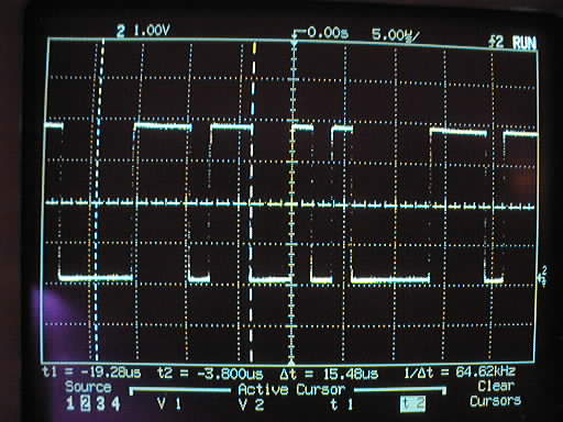
- Find the period of the signal using the automatic feature you played with earlier. Is the value indicated by the scope similar to the one you measure on the screen? Why?
- The best way in such a case is to use cursors to measure the exact timing. Press Cursors in the Measure section at the top left of the panel.
- Press the button next to t1 at the bottom of the screen.
- Turn the knob next to the Cursors button and move the vertical cursor to the first transition of the waveform.
- Press t2 and move the second vertical cursor to the same transition, a period away.
- Note: it is very likely that the waveform will "jump" around as you move the cursor. That's okay. Move it until you can pin it down to the same transition the t1 cursor rests on.
- Look up t1, t2, Delta-t and 1/Delta-t at the bottom of the screen.
              t1 = _______    t2 = _______

              Delta-t = _______ 1/Delta-t = ________
- What is the frequency of the signal?
freq = _________ Hz
- Use the cursors in the same fashion to measure the high and low voltage levels of the waveform. What is the height of the waveform?
V p-p = __________ Volts
- Exercise: Find everything there is to know (frequency, period, voltage peak-to-peak) about the signal present on Test Point #4 of the HP kit.
Part II: Observing instructions on the oscilloscope
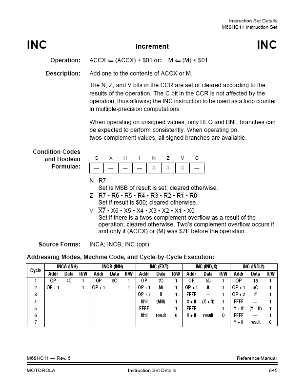
You should have the code of the small program you had to write for this lab. It should be a short loop that increments a byte and stores it at the same address over and over. You will find in tonight's lab that the shorter your program is, the fewer bytes and cycles it uses, the easier it will be to gather information about it.
Enter your program in the kit. Then run it!
The goal of the series of steps below is for you to reconstruct the timing diagram of the execution of the program, while observing only a couple of signals at a time with the oscilloscope.
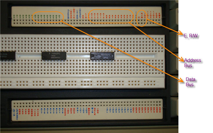
Use the picture below to spot where the different signals are. Note also the location of the GROUND connectors in the lower right corner.
Step 1: The clock signal E
The first signal we want to probe is E, the master clock signal. It is one of several signals generated by the processor that are available from wiring blocks on the kit. E is available on the top row of holes.
Go ahead. Connect Probe 1 to E, ground it, and verify that you can see its regular square wave on the scope.
Step 2: R/W'
The second signal we'll watch along E is R/W'. Connect it to the other probe, ground the probe, and observe the two signals together. Figure out which probe to use as the source so as to get a clear display.
- Which signal is best as the source and why?_______________
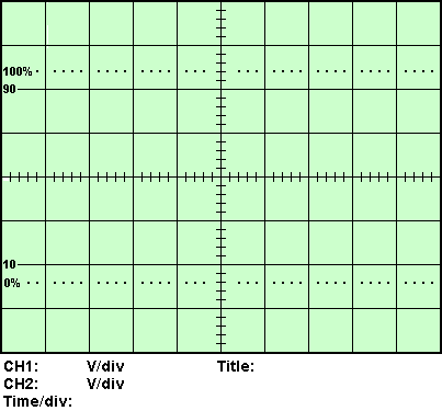
- Record E and R/W' on the timing diagram below, and make sure you record the accurate scales for the voltages (both probe can have different scale factors), and for the time (always the same for both waveforms).
- Remember, measured values should make sense! We are dealing here with a 1MHz processor and signals that oscillate between 0 and 5Volts.
- Can you recognize the infinite loop of your program?
- What element of the display unequivocally defines the loop? ______________
- How long does your loop last?_____________
(Use the scope time-cursors or a function from the time menu to measure this time)
- How often does your loop repeat in one second (here again make the scope give you the answer)? _____________
Step 3: Address Bits
The next step is to observe the behavior of the address bus during the loop. There are 16 bits of addresses, but since your program fits in only a few bytes of memory, most of the memory address bits remain the same during the program. Only the least significant bits change. For this reason we can simplify our task by monitoring the one that changes most: A0. A0 is the least significant bit, and will be 0 when the processor accesses an even address, and 1 otherwise.
- Disconnect one of the two probes (which one, and why?) and connect it to A0. Tweak the holdoff button until you get a clear picture. Use a time scale where each horizontal square on the grid represents one processor cycle, if possible (It won't be possible to have one cycle equal exactly one square, because the processor frequency is not exactly 1MHz, unfortunately)
- Record the behavior of A0 on the timing diagram below, along with the other signal displayed (use two diagrams if your loop lasts longer than 10 cycles.)
Step 4: Data Bits
We will use the same technique to record the behavior of the data bus: we'll only observe D0. Remove the probe from A0 and connect it to D0 and record the behavior of the two waveforms. You will notice that D0 might look very strange compared to other signals... It is in part because it is generated sometimes by the processor, sometimes by the memory, and sometimes neither the processor nor memory is using the data-bus, and the signal is somehow allowed to "float"...
- Question: Why does D0 seem to be both high and low during the short time that R/W' is low, and that it seems impossible to synchronize the scope so as to show D0 in a stable form? Does this happen in other parts of the waveform as well?
Putting it all together
Once the timing diagram is complete, isolate the cycles corresponding to individual instructions, and reconstruct the execution of the instructions in a new timing diagram. Indicate in each cycle what is happening with the processor-memory system, as we have done in class this week.
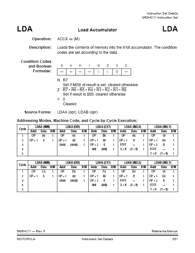
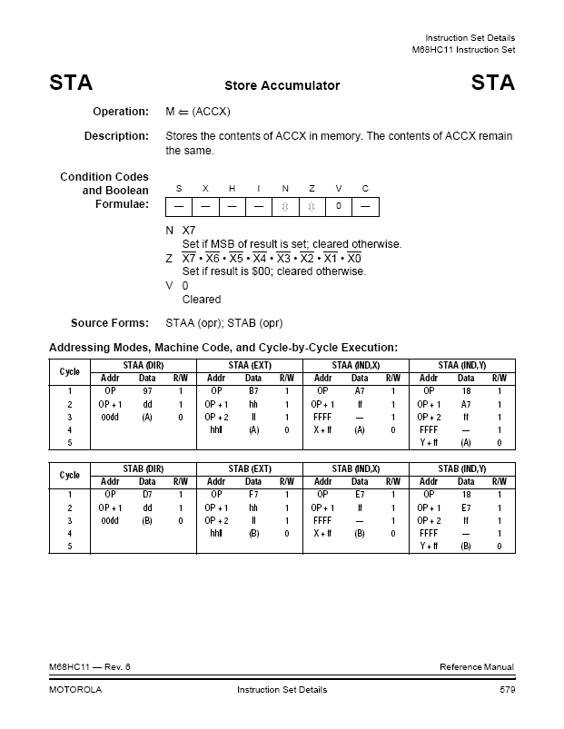
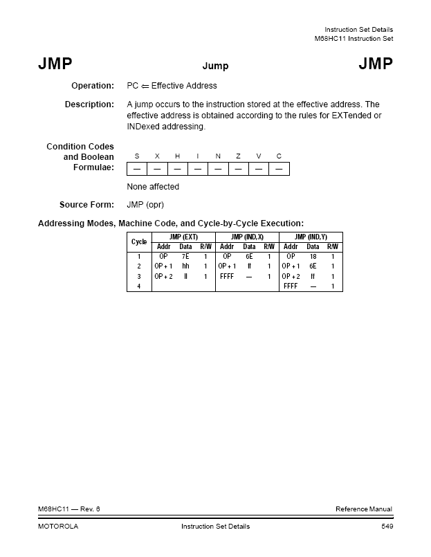
Use the information on the 6811 instructions at the end of this lab to figure out what the processor does during the execution of the instructions. If you are using an instruction that is not in the handout for this lab, simply go to the appendix of the 6811 manual and print the pages you need on your own.
Make sure you clearly highlight the cycles belonging to the different instructions of your program, and write at the bottom of each column what happens during the cycle (e.g. "op code fetch", "1st byte operand fetch", "internal cycle", etc.). Explain why the A0 or D0 bit is high or low during each cycle.
