Difference between revisions of "CSC270 Homework 2 2011"
(→Problem #1) |
(→Problem #1) |
||
| Line 12: | Line 12: | ||
=Problem #1= | =Problem #1= | ||
| − | * Is the gate below a universal gate? It is an AND gate that inverts its input. If a and b are on the other side of the left red wires, the output will be not a and not b. | + | * Is the gate below a ''universal'' gate? It is an AND gate that inverts its input. If a and b are on the other side of the left red wires, the output will be not a and not b. |
<br /> | <br /> | ||
<center>[[Image:notnotand.png]]</center> | <center>[[Image:notnotand.png]]</center> | ||
| + | <br /> | ||
| + | |||
| + | * Make sure you explain why this gate is, or is not, a universal gate. A yes or no answer will not get any credit! | ||
| + | |||
| + | =Problem #2= | ||
| + | |||
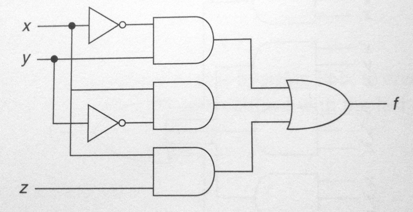
| + | Implement the circuit of Homework #1 with NANDs only. One way to do so is to figure out a way to rewrite the expression for the circuit is such a way that it is a combination of terms of the form not( X and Y ). | ||
| + | <br /> | ||
| + | <center>[[File:CSC270LogicCircuitHomework1.jpg|300px]]</center> | ||
<br /> | <br /> | ||
| − | * | + | |
| + | =Problem 3= | ||
| + | <br /> | ||
| + | <center> | ||
| + | [[Image:CSC270_gates3.gif | 200px]] | ||
| + | </center> | ||
| + | <br /> | ||
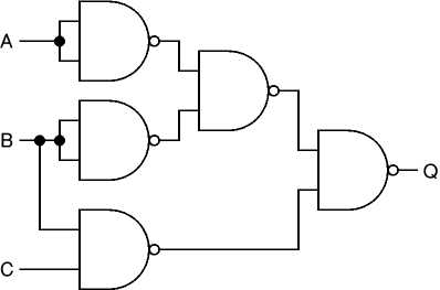
| + | * What is the function Q( A, B, C ) implemented by the circuit shown above, where the gates are NAND gates ? | ||
| + | * What is the diagram of Q using only NOT, OR, and AND gates? | ||
| + | * What is the '''minterm canonical form''' of Q? | ||
| + | * What is its minterm canonical form? | ||
| + | |||
| + | <br /> | ||
| + | <br /> | ||
| + | <br /> | ||
| + | <br /> | ||
| + | <br /> | ||
| + | <br /> | ||
| + | <br /> | ||
| + | <br /> | ||
| + | <br /> | ||
| + | <br /> | ||
| + | <br /> | ||
| + | [[Category:CSC270]][[Category:Homework]] | ||
Revision as of 15:48, 3 February 2011
--D. Thiebaut 15:40, 3 February 2011 (EST)
This assignment deals with minterms, Maxterms, Nands and Nors.
Problem #1
- Is the gate below a universal gate? It is an AND gate that inverts its input. If a and b are on the other side of the left red wires, the output will be not a and not b.

- Make sure you explain why this gate is, or is not, a universal gate. A yes or no answer will not get any credit!
Problem #2
Implement the circuit of Homework #1 with NANDs only. One way to do so is to figure out a way to rewrite the expression for the circuit is such a way that it is a combination of terms of the form not( X and Y ).

Problem 3
- What is the function Q( A, B, C ) implemented by the circuit shown above, where the gates are NAND gates ?
- What is the diagram of Q using only NOT, OR, and AND gates?
- What is the minterm canonical form of Q?
- What is its minterm canonical form?

