Difference between revisions of "CSC270 Lab 11 2011"
(→Designing a 1-bit input I/O controller) |
(→Designing a 1-bit input I/O controller) |
||
| Line 100: | Line 100: | ||
expect. | expect. | ||
| + | ===Step 6: Understanding Address Decoding=== | ||
| − | ===Step | + | * Modify your program and change only the address of the I/O Port to a different Hex value, and demonstrate that your setup still continues to work, even though you are now using LDAA and STAA instructions with a different address for the I/O port. |
| + | |||
| + | * How many different such addresses exist? In other words, how many different addresses energize the Yi output that you use to enable your I/O port? | ||
| + | |||
| + | ===Step 7: More Programming=== | ||
* Write a program that makes the LED blink (choose | * Write a program that makes the LED blink (choose | ||
Revision as of 08:50, 11 April 2011
--D. Thiebaut 22:11, 10 April 2011 (EDT)
Contents
Designing a 1-bit input I/O controller
Today you have a simple design to implement, but you should make sure you go through the steps carefully, as a flaw in the design could kill some of the kit's components.
This lab assumes that you have assembled, designed and fully tested the 1-bit output controller from Lab #10.
Step 1: Basic Design
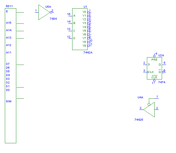
Complete the address decoding part of the schematics below, using the approach we took during the class period.
Connect the E and address bits to the decoder the exact same way you did in the last Lab, so that you will not have to change the wiring on your kit.
What hexadecimal address did you assign to your flipflop in Lab 10?____________
What Yi output is activated by this address? _________
This is the same address we will use for your 1-bit input. We can use the same address for both ports, the input port and the output port, because in the new design the output port (flipflop) is energized only when R/W is low (the processor writes the bit to the flipflop), and the input port you are building tonight will be energized only when R/W is high (the processor will read the bit generated by the switch).
Draw the timing diagrams for a STAA XXXX and a LDAA XXXX instruction, where XXXX is the address you picked for the I/O port. Make sure you show E, the Address bus, R/W, D0, the clock input of the flipflop, and the active-low enable of the tri-state driver.
Step 2: Wiring
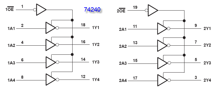
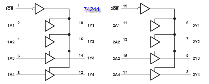
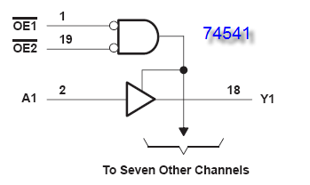
Rewire your kit so that it matches your design. HOWEVER, DO NOT CONNECT THE OUTPUT OF THE TRI-STATE DRIVER TO D0. We will do this only when we are sure your circuit is wired correctly. You have several tri-state drivers available to you to choose from:
Pick the one that works best for your design.
Step 3: Programming
- Write an endless loop that will constantly read a byte (your interested in 1 bit, but you have to get a whole byte none-the-less) at the address
corresponding to your 1-bit input port, and write it back at the same address, storing it in the 1-bit flipflop.
- Assemble the program, and enter it in your kit.
- Run the program.
- Use the scope and verify that the Yi output of the decoder that you are
currently using for your 1-bit flipflop is energized by your program.
- It should look something like this:
- Monitor the R/W signal as well, and watch both the Yi output and R/W'.
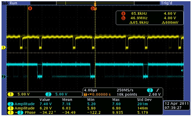
You should observe something similar (though not exactly equal) to the following picture:
Explain why you see a R/W pulse only every other Yi pulse. Make sure you indicate which signal is which on your scope captures!
Step 4: First-Phase Testing
Do NOT connect the output of the driver to D0 yet!
- Connect the enable input(s) of your driver to the oscilloscope and
observe it/them along with R/W and your Yi signal (use 3 probes).
- Verify that your driver is turned
ON only when R/W is high and Yi is low. You shouldn't connect the data output of your driver to the data bus (bit D0) until you are sure that the gate is activated at the correct time, under correct conditions. Failure to do this will result in the destruction of some chips (either the ones on your breadboard, or the ones inside the kit), so, please, be careful!
Step 5: Connection to Data-Bus
- Once you have observed and verified the correct timing of the signals, connect the output of
the driver to D0, and its input to one of the switches.
- Activate the switch (you might want to use a tiny screwdriver), and verify that
the LED turns ON or OFF according to the position of the switch, as we should expect.
Step 6: Understanding Address Decoding
- Modify your program and change only the address of the I/O Port to a different Hex value, and demonstrate that your setup still continues to work, even though you are now using LDAA and STAA instructions with a different address for the I/O port.
- How many different such addresses exist? In other words, how many different addresses energize the Yi output that you use to enable your I/O port?
Step 7: More Programming
- Write a program that makes the LED blink (choose
whatever blinking frequency you wish) when the switch is in one position, and that turns the LED OFF when the switch is in the opposite position.
- Again, demonstrate the correct operation of your program, please!
