Difference between revisions of "CSC270 Homework 4 2012"
(→Problem #2) |
(→Problem #2) |
||
| Line 18: | Line 18: | ||
</center> | </center> | ||
<br /> | <br /> | ||
| − | Given the circuit above, which uses 74LS74 D flip-flops, complete the timing diagram below and show how Q0, Q1 and Q2 behave as a function of time. | + | Given the circuit above, which uses 74LS74 D flip-flops, complete the timing diagram below and show how Q0, Q1 and Q2 behave as a function of time. Assume that the timing diagram below shows the time the circuits were powered-up at the left end of the time axes. |
<br /> | <br /> | ||
<center>[[Image:CSC270TimingDiagramDClock.png|500px]] | <center>[[Image:CSC270TimingDiagramDClock.png|500px]] | ||
Revision as of 17:25, 22 February 2012
--D. Thiebaut 17:23, 22 February 2012 (EST)
This assignment is due on 2/29/12 at 1:10 p.m.
Problem #1
Can one build an RS flip-flop using one NAND and one NOR, wired together in a feedback loop, similar to the NAND-NAND or NOR-NOR RS flip-flop?
Why, or why not?
Problem #2
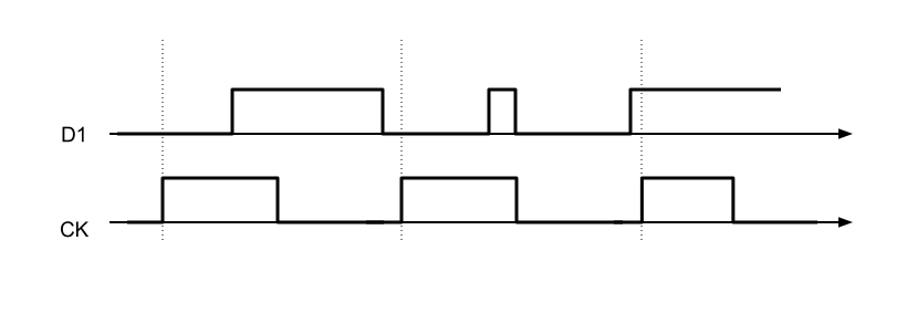
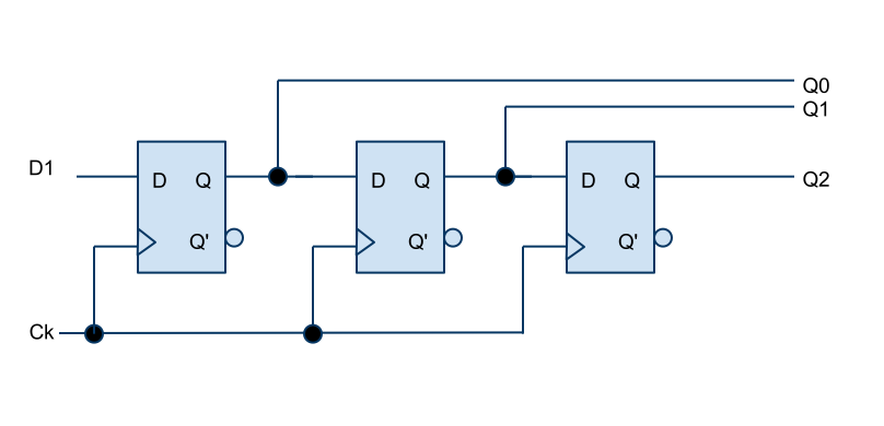
Given the circuit above, which uses 74LS74 D flip-flops, complete the timing diagram below and show how Q0, Q1 and Q2 behave as a function of time. Assume that the timing diagram below shows the time the circuits were powered-up at the left end of the time axes.

