Difference between revisions of "CSC231 Logic Design Lab 2014"
(→EXPERIMENT #2: INTEGRATED CIRCUITS AND LOGIC GATES) |
(→Data Sheets) |
||
| Line 11: | Line 11: | ||
| − | |||
| − | |||
| − | |||
| − | |||
| − | |||
| − | |||
| − | |||
| − | |||
==EXPERIMENT #1: INVESTIGATING THE KIT== | ==EXPERIMENT #1: INVESTIGATING THE KIT== | ||
<br /> | <br /> | ||
Revision as of 10:42, 19 November 2014
--D. Thiebaut (talk) 10:35, 19 November 2014 (EST)
Contents
Logic Design LAB
EXPERIMENT #1: INVESTIGATING THE KIT
Overview of the Kit
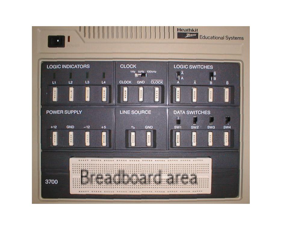
The main tools for us today are the switches, the LEDs, the +5 and GND wiring plots, and the breadboard area.
Exploration
For this part, concentrate only on the flatter part of the Digital Kit, not the circuit board that is upright, facing you. Please follow the steps below.
- Power OFF. Always turn OFF the power when you are wiring circuits. This will prevent shorts and extend the life of your circuits.
- Connect a wire between the Logic Indicator L4 and the Logic Switch A.
- Power ON
- Activate Switch A, and observe the LED (Light Emitting Diode) turn ON and OFF.
- Power OFF
- Switch the wire from A to A-Bar, turn the power back ON, and see how the LED reacts .
- Same experiment, but this time replace the Logic Switch by one of the Data Switches.
- Power OFF.
- Connect one of the Logic Indicators to the Clock signal. Connect a second wire from another Logic Indicator to the Clock-bar signal. Make sure the sliding switch is on the 1Hz mark.
- Power UP. What do you observe?
- Slide the switch to 1KHz. What happens? Why? Is there any difference in the brightness of the LED? Why?
EXPERIMENT #2: INTEGRATED CIRCUITS AND LOGIC GATES
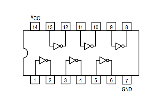
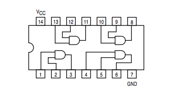
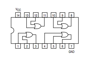
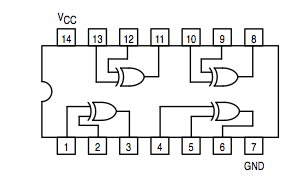
You should have the data sheets of the integrated circuits implementing the AND gate (74LS08), the OR gate (74LS32), and the XOR gate (74LS86). The XOR is not and universal gate, but its function is encountered enough times in the real world that manufacturers have built a circuit just for this function. The equation for a XOR b is ( a and not b ) or ( not a and b), which can be implemented using the simple AND, OR, and NOT.
You will be given three circuits in class, with a piece of tape hiding its part number. The circuits are labeled A, B, and C. Your job is to
- pick one gate of the circuit,
- wire up the inputs of the gate to switches,
- attach the output of the gate to an LED,
- activate the different inputs
- figure out which circuit contains AND gates, which contains OR gates, and which contains XOR gates.
Use the information shown in the Figure 1 to help you wire the circuit.
- Rule 1
- Always make sure the notch on the circuit is facing left. This way the circuit matches the diagram on the datasheets.
- Rule 2
- Always make sure that the circuit is connected to +5V through its pin 14, and to GND via its pin 7.
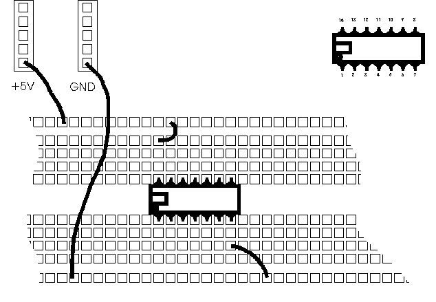
Figure 1:Wiring of an IC on the breadboard. Always identify pin 1 of the IC which is on the left (or below) the notch or circle embossed on the top of the chip
You may find the tables below useful for keeping notes of what is going on.
| Input 1 | Input 2 | Output |
|---|---|---|
|
|
|
|
| 0 | 0 | |
| 0 | 1 | |
| 1 | 0 | |
| 1 | 1 |
| Input 1 | Input 2 | Output |
|---|---|---|
|
|
|
|
| 0 | 0 | |
| 0 | 1 | |
| 1 | 0 | |
| 1 | 1 |
| Input 1 | Input 2 | Output |
|---|---|---|
|
|
|
|
| 0 | 0 | |
| 0 | 1 | |
| 1 | 0 | |
| 1 | 1 |
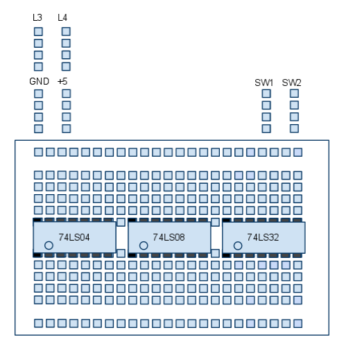
- We'll explore in class how to verify the property, both theoretically, on paper, and practically, using digital electronic circuits. The diagram below needs to be completed in class before wiring and testing.
Useful Gates
|
Inverter: 74LS04 | |
|
AND gate: 74LS08 | |
|
OR gate: 74LS32 | |
|
Exclusive OR: 74LS86 |
EXPERIMENT #3: A 2-BIT ADDER
| a | b | Output |
|---|---|---|
|
|
|
|
| 0 | 0 | |
| 0 | 1 | |
| 1 | 0 | |
| 1 | 1 |
EXPERIMENT #4: BOOLEAN ALGEBRA
For those who have taken CSC231, your job for today is to use AND, OR, and NOT gates and show that they are designed following the axioms of the Boolean Algebra.
- Get together as a group and discuss the axioms of a Boolean Algebra shown below (and taken from Wikipedia)
a OR (b OR c) = (a OR b) OR c a AND (b AND c) = (a AND b) AND c Associativity a OR b = b OR a a AND b = b AND a Commutativity a OR (a AND b) = a a AND (a OR b) = a Absorption a OR (b AND c) = (a OR b) AND (a OR c) a AND (b OR c) = (a AND b) OR (a AND c) Distributivity a OR NOT a = 1 a AND NOT a = 0 Complements
- Figure out how to test each axiom
- Divide the work to be done into tasks and assign each task to a group or to an individual
- Demonstrate to the class that the gates found in the integrated circuits used in the lab verify the axioms of the Boolean Algebra.
EXPERIMENT #5: CIRCUIT WIRING
Build a circuit implementing the function f(a, b, c) = Σ(1, 2, 3, 5, 7).
Note: you might want to try to simplify f as much as you can, since the simpler f becomes, the simpler your hardware will be!
Generate the truth table for your circuit and verify that it generates a 1 for Minterm 1, Minterm 2, Minterm 3, Minterm 5, and Minterm 7.
LAB REPORT
That's it for this lab! Translate your notes into a lab report that you will hand in next Wednesday. The first lab report will be graded generously, and you will get feedback that will help you better organize the next reports (if necessary).
When preparing your lab reports, keep these important points in mind:
- Your lab should bear your name, and the date of the lab.
- Your lab report should be self-contained. Somebody should be able to redo the same experiments using the information contained in your report. Including the original Web page for the lab, or cutting and pasting from the Lab Web page into your report are good and welcomed ideas.
- You may type or hand-write your report. If you have a lot of diagrams, hand-generating them might be faster than using a drawing package.
- Record and report observations truthfully. If you measure a signal to be of a value different from the value you think, or know it should have, report the value that you measure, not the value that you believe you should have measured. You should comment on the measurement and indicate why you think the value is incorrect.
- The Web documents for this class contain many graphic files showing different types of circuit and designs. Do not hesitate to use them to illustrate your own documents.
- A report should be an honest log of your work, not an idealized version of it.
- Use the KISS philosophy: "Keep it simple, Stupid!"
- When drawing schematics, make sure you try to follow these conventions:
- Signals flow from left to right
- All gates are nicely drawn (by hand or with a CAD package), and each pin is labeled with its pin number on the chip.
- The Vcc and Ground pins are indicated.
- Input and output signals are clearly labeled
- The part number is written inside or next to the gates (08 for an AND gate, 32 for an OR gate, etc.)
- You may find Allie's Lab 8 report from a couple years ago an interesting model to look at: Lab example. Note the very nice use of pictures taken during the lab to document the report. Note that Allie is a very prolific writer, and her report might be on the longer side! :-)
- The report will count as a regular homework assignment.
