CSC103 Lab 2012
--D. Thiebaut 12:40, 5 February 2012 (EST)
-
<meta name="keywords" content="computer science, How Computers Work, Dominique Thiebaut, smith college" /> <meta name="description" content="Dominique Thiebaut's Web Page" /> <meta name="title" content="Dominique Thiebaut -- Computer Science" /> <meta name="abstract" content="Dominique Thiebaut's Computer Science Web pages" /> <meta name="author" content="thiebaut at cs.smith.edu" /> <meta name="distribution" content="Global" /> <meta name="revisit-after" content="10 days" /> <meta name="copyright" content="(c) D. Thiebaut 2000, 2001, 2002, 2003, 2004, 2005, 2006, 2007,2008" /> <meta name="robots" content="FOLLOW,INDEX" />
Contents
This lab is about logic design. Work in pairs and alternate with your lab partner when working at the keyboard. You do not have to turn in anything at the end of the lab. The goal of the lab is to get you to play with a logic gate simulator.
Logic Simulator
Reference
- You can find a nice description of the simulator used in this lab at http://math.hws.edu/TMCM/java/xLogicCircuits/
The Applet
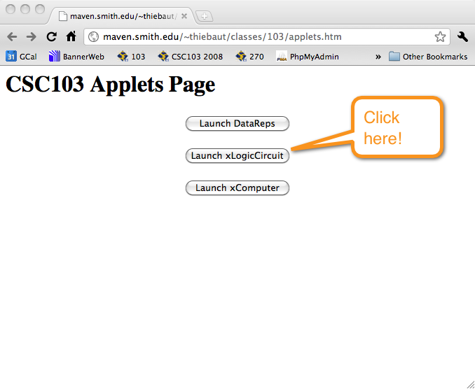
- Go to this page ( or this one if the previous one seems slow to load up) and click on the middle button: "Launch xLogicCircuit" and wait for the simulator to show up.
- You should see this window:
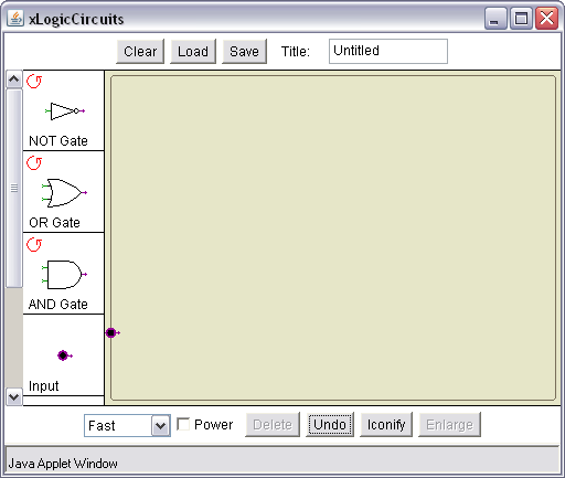
NOT, OR, and AND gates
Study all three fundamental gates: the NOT gate, the OR gate, and the AND gate.
The NOT gate
- Drag an input symbol on the leftmost part of the wiring area
- Drag an output symbol on the rightmost part of the wiring area
- Drag a NOT gate in the middle of the area
- Connect the input symbol to the input of the NOT gate with a wire (left click and drag), and the output of the NOt gate to the output symbol with another wire
- Turn the power on (bottom of the window)
- Left-click on the input symbol to generate a 1 (red) or a zero (blue). Try all possible variations of the input and verify that the output symbol is always the opposite of the input value.
Remember that you can drag symbols around by right-clicking on them.
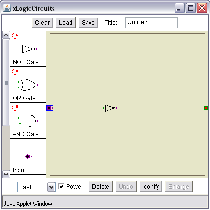
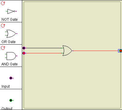
Once you're done, clear your wiring area and wire up an OR gate, as shown below:
The OR gate
Take the similar steps as you did for the NOT gate, and wire up an OR gate with 2 inputs. Try all possible combinations of the two inputs and verify that it's truth table is the following one:
| input1 | input2 | input1 OR input2 |
| 0 | 0 | 0 |
| 0 | 1 | 1 |
| 1 | 0 | 1 |
| 1 | 1 | 1 |
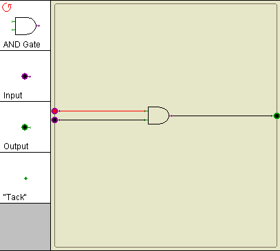
The AND gate
Take the similar steps as you did for the OR gate, and wire up an AND gate with 2 inputs. Try all possible combinatins of the two inputs and verify that it's truth table is the following one:
| input1 | input2 | input1 OR input2 |
| 0 | 0 | 0 |
| 0 | 1 | 0 |
| 1 | 0 | 0 |
| 1 | 1 | 1 |
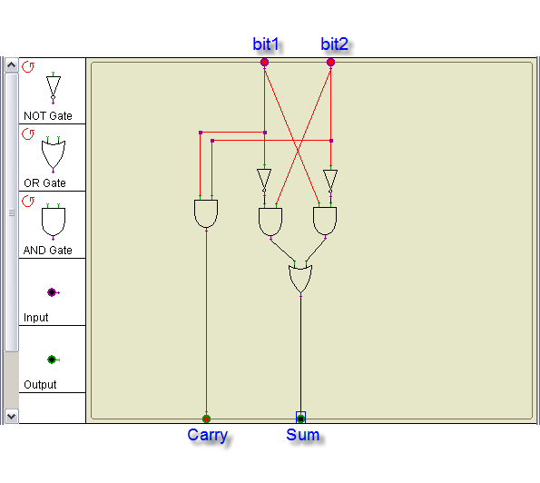
Binary Adder
Wire up the circuit of the binary adder which we have seen in class.
Try all possible combinations of the inputs, and verify that the outputs correspond to the sum of the two inputs, in binary.
| bit1 | + | bit2 | = | carry | sum | |
|---|---|---|---|---|---|---|
| 0 | + | 0 | = | 0 | 0 | |
| 0 | + | 1 | = | 0 | 1 | |
| 1 | + | 0 | = | 0 | 1 | |
| 1 | + | 1 | = | 1 | 0 |
3-Bit Adder
- A 3-bit adder is a circuit with 3 inputs, or bits, and two outputs, corresponding to the carry and the sum, as for the 2-bit adder.
- On a piece of paper, write the truth table for the 3-bit adder.
| b1 | b2 | b3 | carry | sum |
| 0 | 0 | 0 | ||
| 0 | 0 | 1 | ||
| 0 | 1 | 0 | ||
| 0 | 1 | 1 | ||
| 1 | 0 | 0 | ||
| 1 | 0 | 1 | ||
| 1 | 1 | 0 | ||
| 1 | 1 | 1 |
- Use the simulator to verify that the logic expression for the carry bit is
carry = ( a and b ) or ( a and c ) or ( b and c )
- Once you have wired and tested it, demonstrate it to your instructor, please! :-)
Hope you enjoyed the lab!
