CSC270 Lab 1 2011
Contents
LAB #1
© D. Thiebaut, 2009
The lab is in two parts tonight, mostly because students who have taken CSC231 have already some knowledge of the digital training kit. So, for tonight, follow this path, depending on your background:
- if you haven't taken CSC231, please do TBA
- if you have taken CSC231, concentrate on TBA
Data Sheets
If you need to refer to the data sheets of various chips during the lab, you can click on any of the links below: If the datasheet haven't been printed yet, print a set from these links: 74LS00 74LS01 74LS02 74LS03 74LS04 74LS05 74LS08 74LS09 74LS10 74LS12 74LS13 74LS15 74LS20 74LS21 74LS22 74LS26 74LS27 74LS28 74LS30 74LS32 74LS33 74LS37 74LS38 74LS40 74LS42 74LS47 74LS48 74LS51 74LS54 74LS55 74LS74 74LS75 74LS76 74LS83 74LS85 74LS86 74LS90 74LS9 74LS13 74HCT24 74LS24 74HCT24 74LS25 74HCT54.
EXPERIMENT 1: Investigating the Digital Training Kit
For this part, concentrate only on the flatter part of the Digital Kit, not the circuit board that is upright, facing you. Please follow the steps below.
- Power OFF. Connect a wire between the Logic Indicator L4 and the Logic Switch A. Activate Switch A, and observe the LED (Light Emitting Diode) turn ON and OFF. Switch the wire from A to A-Bar, and see how the LED reacts .
- Power OFF. Same experiment, but this time replace the Logic Switch by one of the Data Switches.
- Power OFF. Connect one of the Logic Indicators to the Clock signal. Connect a second wire from another Logic Indicator to the Clock-bar signal. Make sure the sliding switch is on the 1Hz mark. Power UP. What do you observe?
- Slide the switch to 1KHz. What happens? Why? Is there any difference in the brightness of the LED? Why?
EXPERIMENT 2: INTEGRATED CIRCUITS AND LOGIC GATES
You should have the data sheets of the integrated circuits implementing the AND gate (74LS08), the OR gate (74LS32), and the XOR gate (74LS86). The XOR is not and elementary gate, but its function is encountered enough times in the real world that manufacturers have built a circuit just for this function. The equation for a XOR b is ( a and not b ) or ( not a and b), which can be implemented using the simple AND, OR, and NOT.
You will be given three circuits in class, with a piece of tape hiding its part number. The circuits are labeled A, B, and C. Your job is to
- pick one gate of the circuit,
- wire up the inputs of the gate to switches,
- attach the output of the gate to an LED,
- activate the different inputs
- figure out which circuit contains AND gates, which contains OR gates, and which contains XOR gates.
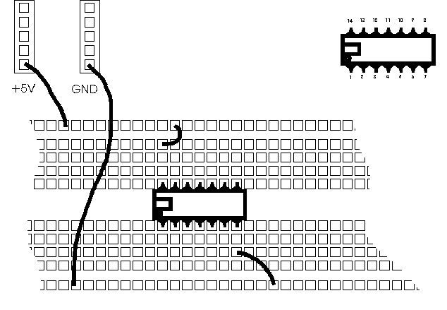
Use the information shown in the Figure 1 to help you wire the circuit. Always make sure that the circuit is connected to +5V through its pin 14, and to GND via its pin 7.

Figure 1:Wiring of an IC on the breadboard. Always identify pin 1 of the IC which is on the left (or below) the notch or circle embossed on the top of the chip
You may find the tables below useful for keeping notes of what is going on.
| Input 1 | Input 2 | Output |
|---|---|---|
|
|
|
|
| 0 | 0 | |
| 0 | 1 | |
| 1 | 0 | |
| 1 | 1 |
| Input 1 | Input 2 | Output |
|---|---|---|
|
|
|
|
| 0 | 0 | |
| 0 | 1 | |
| 1 | 0 | |
| 1 | 1 |
| Input 1 | Input 2 | Output |
|---|---|---|
|
|
|
|
| 0 | 0 | |
| 0 | 1 | |
| 1 | 0 | |
| 1 | 1 |
EXPERIMENT #3: MYSTERY CIRCUIT
Get a new circuit from your instructor, one that will also have its part number hidden, and which is labeled D. The gates inside are wired similarly as the gates in Circuits A, B, and C.
Energize one of the gates and figure out what logic function is performed by the gate.
| Input 1 | Input 2 | Output |
|---|---|---|
|
|
|
|
| 0 | 0 | |
| 0 | 1 | |
| 1 | 0 | |
| 1 | 1 |
EXPERIMENT #4: BOOLEAN ALGEBRA
For those who have taken CSC231, your job for tonight is to use AND, OR, and NOT gates and show that they are designed following the axioms of the Boolean Algebra.
- Get together as a group and discuss the axioms of a Boolean Algebra shown below (and taken from Wikipedia)
<math>a \lor (b \lor c) = (a \lor b) \lor c</math> <math>a \land (b \land c) = (a \land b) \land c</math> associativity <math>a \lor b = b \lor a</math> <math>a \land b = b \land a</math> commutativity <math>a \lor (a \land b) = a</math> <math>a \land (a \lor b) = a</math> absorption <math>a \lor (b \land c) = (a \lor b) \land (a \lor c)</math> <math>a \land (b \lor c) = (a \land b) \lor (a \land c)</math> distributivity <math>a \lor {\neg}a = 1</math> <math>a \land {\neg}a = 0</math> complements
The next experiment for this lab is to wire up a two-bit adder. It will have two inputs, A and B, and two outputs, SUM and CARRY. First fill out the truth table below, where SUM and CARRY are the two functions that you need to implement, and that represent the arithmetic sum of the two inputs.
| A | B | Carry | Sum |
|---|---|---|---|
|
|
|
|
|
| 0 | 0 | ||
| 0 | 1 | ||
| 1 | 0 | ||
| 1 | 1 |
- Now that you have the truth tables, find the logic expressions (equations) for SUM and CARRY that we developed in class.
- Next, draw the logic diagram for SUM and CARRY using any gates you think will simplify the overall diagram. Draw the logic diagrams cleanly, and do not hesitate to make them large, as you will need to add more information to them.
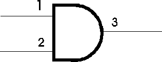
- Identify the circuits numbers (e.g. 7408) corresponding to your logic gates, and write these numbers inside or right next to the gates in your diagram. Then identify which gate in the circuit you will be using, and write the pin-numbers next to the inputs and outputs. The figure below shows an example of how one would label an AND gate, assuming that we use the first AND of a 7408, with inputs on pins 1 and 2, and output on pin 3.
- When you are done labeling all the gates in this fashion, put the ICs you need on the breadboard, the notch to the left, and turn the power OFF. Connect the chips' power and gnd pins to +5 and GND.
- Then add wires between the gates, making the connections that you have shown on your diagram. As you add wires, highlight or redraw in bold the corresponding lines in your logic diagram, so that you can easily see which connections are made and which ones are left. Make sure you generate the A and B inputs from data switches, and that you connect the SUM and CARRY outputs to Logic Indicators.
- Turn the power on, and test your circuit. Does it add?
MAJORITY VOTER
If you have time, build a majority voter. A majority voter is a circuit with 3 inputs that outputs what the majority of the inputs represent. In other words, if 2 or more of the inputs are 1, the output is 1. If 2 or more of the inputs are 0, the output is 0.
LAB REPORT
You have to write a lab report for this lab. The key part of a lab report is that it should be self-contained. The answer to a question may not be very useful if the question is not also part of the report. Ideally, a good lab report should be all that is needed for someone else to repeat all the experiments.
A simple way to accomplish this is to use the text of this Web page as appendix to your report, or to simply cut and paste the various sections of the lab into your typed report. This is not cheating: it's just documenting the experiment you had to perform. Then you write up your observations and results. Usually a paragraph a 3 to 5 lines is sufficient for most answers.
If an experiment does not work, report the experiment as you experienced it, and do not guess what you think should have happened.
Your lab report is due a week after the lab is performed. In this case, a week after the engineering question is fully covered in class. Even if we answer all the questions in class, you should report them in your report.
The report will count as a regular homework assignment.
