Xilinx ISE Schematics Sequential Circuit
--D. Thiebaut 13:47, 23 April 2012 (EDT)
This lab illustrates how to create a sequential circuit for the Xilinx CoolRunner II CPLD, and how to perform a behavioral simulation of it.
Contents
Introduction
This lab assumes you have gone through the previous lab in this series.
In this lab we will be using flip-flops. Xilinx offers a large library of sequential circuits. Make sure to check it out when searching for circuits: Xilinx Refernce Library.
The Circuit of the Day
The circuit we want to implement in this lab is a sequential circuit controlling 3 LEDs, one Green, on Yellow, and one Red that stay on for one cycle of the clock in the following fashion:
- When the outside command signal called cmd is 1, the cycling goes Green, Yellow, Red, Green, Yellow, etc...
- When the outside command cmd is 0, the cycling stops on Red. If cmd is activated when the light that is on is not Red, the cycling still follows the Green-Yellow-Red path, and stops on Red as long as cmd remains 0.
Generate the equation for this 2-flip-flop circuit and its outputs (R, G, and Y).
D0 = cmd and not( Q1 ) and not( Q0 )
D1 = not( Q1 ) and Q0
R = not( Q1 or Q0)
Y = Q1
G = not( R + Y )
Illustrated Steps
Schematics
- Create a new project called GYRSequencer.
- Create a new source with type schematics, and call it Sequencer.
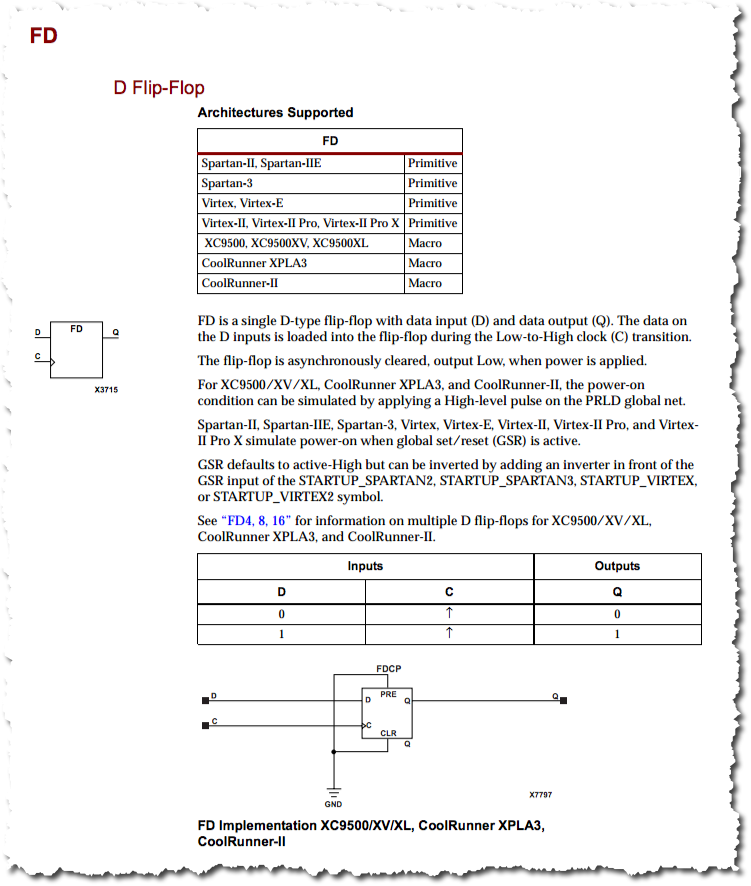
- Xilinx supports many different flip-flop models, some with active low signals, some with negative edge clocks. You can find them all in the Xilinx Library Manual (in pdf form). We'll pick the FD flip-flop for this lab:

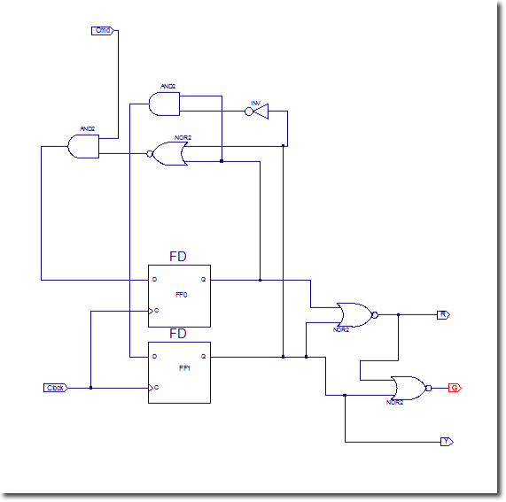
- Create your schematics, according to the equations you obtained from your previous analysis.
- Note: You can rotate gates by using Ctrl-R on the keyboard.
- Make sure you add an input marker for the clock signal.
- Tip
- You can verify that a set of wires are connected properly by using cursor mode (you click on the cursor arrow in the vertical menu) and clicking on one of the wires. Every wire connected to that wire, including this wire, will turn red.
- Here's the (not so pretty) circuit we get, given our equations.

- Synthesize your circuit (in Impement Design menu of options). Continue only if your synthesis is successful. Otherwise figure out what the bugs are from the error log in the console window.
Verilog Test Module
- Create a New Source file, of type Verilog Test Fixture.
- Call it Test (or whatever name makes good sense to you).
- Edit the initial module to look something like the code below:
// Verilog test fixture [...] - Tue Apr 24 15:25:45 2012

`timescale 1ns / 1ps

module Sequencer_Sequencer_sch_tb();

// Inputs
   reg Cmd;
   reg Clock;

// Output
   wire Y;
   wire R;
   wire G;

// vars
   integer i;

// Instantiate the UUT
   Sequencer UUT (
		.Cmd(Cmd),
		.Y(Y),
		.R(R),
		.Clock(Clock),
		.G(G)
   );

	// setup the clock to switch every 10 ns
	initial begin
		Cmd = 0;
		Clock = 0;
	end

	initial begin
	// wait 100 ns
		#100

	// flip clock every 10 ns
		forever begin
			#10 Clock = ~Clock;
		end
	end

	// activate the cmd signal regularly
	always @ ( Cmd or Clock )
		#100
		for ( i = 0; i < 200; i = i+1 )
			begin
			#7  if ( i % 30 == 0 ) Cmd = ~Cmd;
			end

endmodule
- Do a Behavioral Check Syntax to test the syntax of your Verilog test module.
- Run the Behavioral Simulation Model
- Adjust the scale and the ordering of the signal to your liking, and verify that you get something similar to the waveforms below:

Challenge of the Day |
Our design for this 3-state sequencer has a transient state. When Q1 and Q0 are 1 1, the system is in State 3, for which Yellow is 1, and it should automatically bring the FSM to State 0, where Red should be 1. We cannot verify its correct behavior, unless we find a way to force Q1 and Q0 to 1.
One way to do this is to modify the schematics and use different flip-flop designs that have a Preset input, and modify the Verilog test module to activate this Preset at the right times.
