CSC270 Lab 8
--D. Thiebaut 14:36, 8 April 2009 (UTC)
This lab will take you through the steps required to build a 1-bit output port with the 6811 Kit.
Setup
The figure below contains all the main players for tonight.
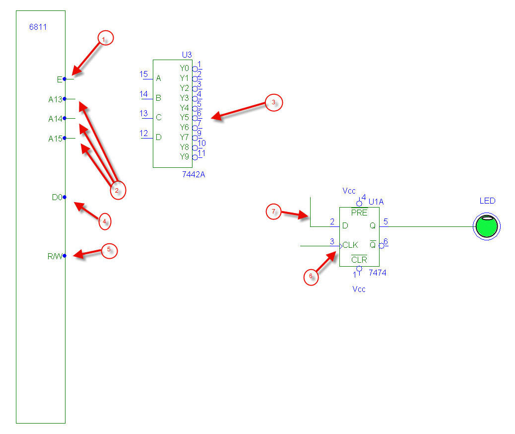
You have to figure out the missing areas, with a little bit of help:
- 1. E. The clock. You are going to use it to enable the decoder to operate only during the second half of a cycle, when all the signals are stable. E is low in the first half of the cycle, and is high in the second half.
- The only problem is that the 7442 decoder that we have available to us is a 4-to-10 decoder without an Enable input... Keep on reading...
- 2. The Address bits A15, A14, A13. Somehow we should connect them along with E to the decoder so that we can recognize an address in the range 7000 to AFFF during the second half of a cycle.
Figure out a way to connect E, A15, A14, and A13 to the decoder inputs so that one of the Yi outputs is activated for an address that you will have selected in the range 7000 to AFFF. Make sure that the Y output you selected is not activated by any address lower than 7000 (remember our "bug" in this morning's lecture), or by an address higher than AFFF.
                        address                  Yi activated by this address
                        ________                 _____________________________

                        6000 (RAM)                   Y_

                        7000 (avail)                 Y_

                        8000 (avail)                 Y_

                        9000 (avail)                 Y_

                        A000 (uP IO)                 Y_
Get a copy of the datasheet of the 7442 decoder...
- 3. There isn't one unique answer for the selection of Yi. Depending on how you connect the A15, A14, A13 and E signals to the decoder, you may end up with a Yi that is not the same as the Yi another team will have selected during this lab. You now need to use the Yi active-low output that you have selected and combine it with R/W to generate a negative pulse for the clock signal of the flip-flop.
- Complete the timing diagram below showing the shape of the different signals when the processor is writing at the address you selected as the address of your I/O device.
                                   ---+             +-------------+
                                      |             |             |
                   E  ________________+=============+_____________+============_______

                   Address            :                           :
                   Bus _______________________________________________________________

                                      :                           :
                  R/W ________________________________________________________________

                                      :                           :
                  Yi  ________________________________________________________________

                  7474                :                           :
                  Clock ______________________________________________________________
- 4. This step should be straightforward. Connect the D0 output of the data bus to the data input of your flipflop...
- 5. You should know what to do with R/W after Step 3!
- 6. Same remark. The 7474 clock input should now be connected to a gate that receive R/W and your Yi signal.
- 7. This step should have been taken care of in Step 4 above. Make sure you get your instructor to verify your schematics before you start wiring things up.
Testing your circuit
Wire up your circuit. Make sure you put the 7442 to the leftmost part of the breadboard, as you will be reusing it in the last two labs of this semester. For this reason make sure you keep the 7442 wired up at the end of the lab tonight, and tag the kit with your name before you leave so that you won't have to rewire the decoder next time.
Write a simple endless loop that repeatedly write 0, then 1, then 0, then 1, etc., in your 1-bit flipflop. Assemble it, enter it in the kit, and run it.
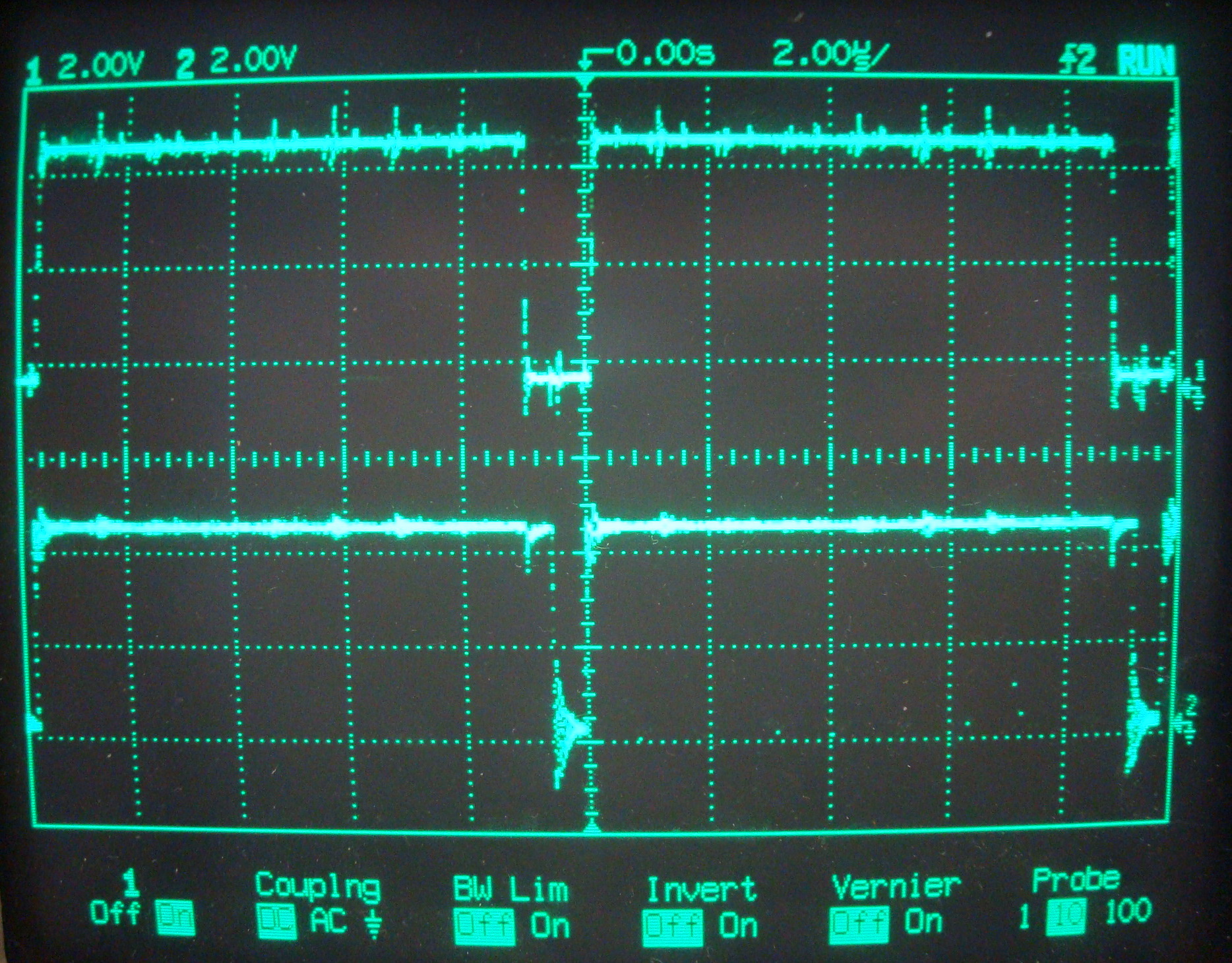
Use the scope and take a look at R/W and your Yi output.
Verify that you see something like this:

In your report, explain which signal is which, and why this timing diagram is the correct one.
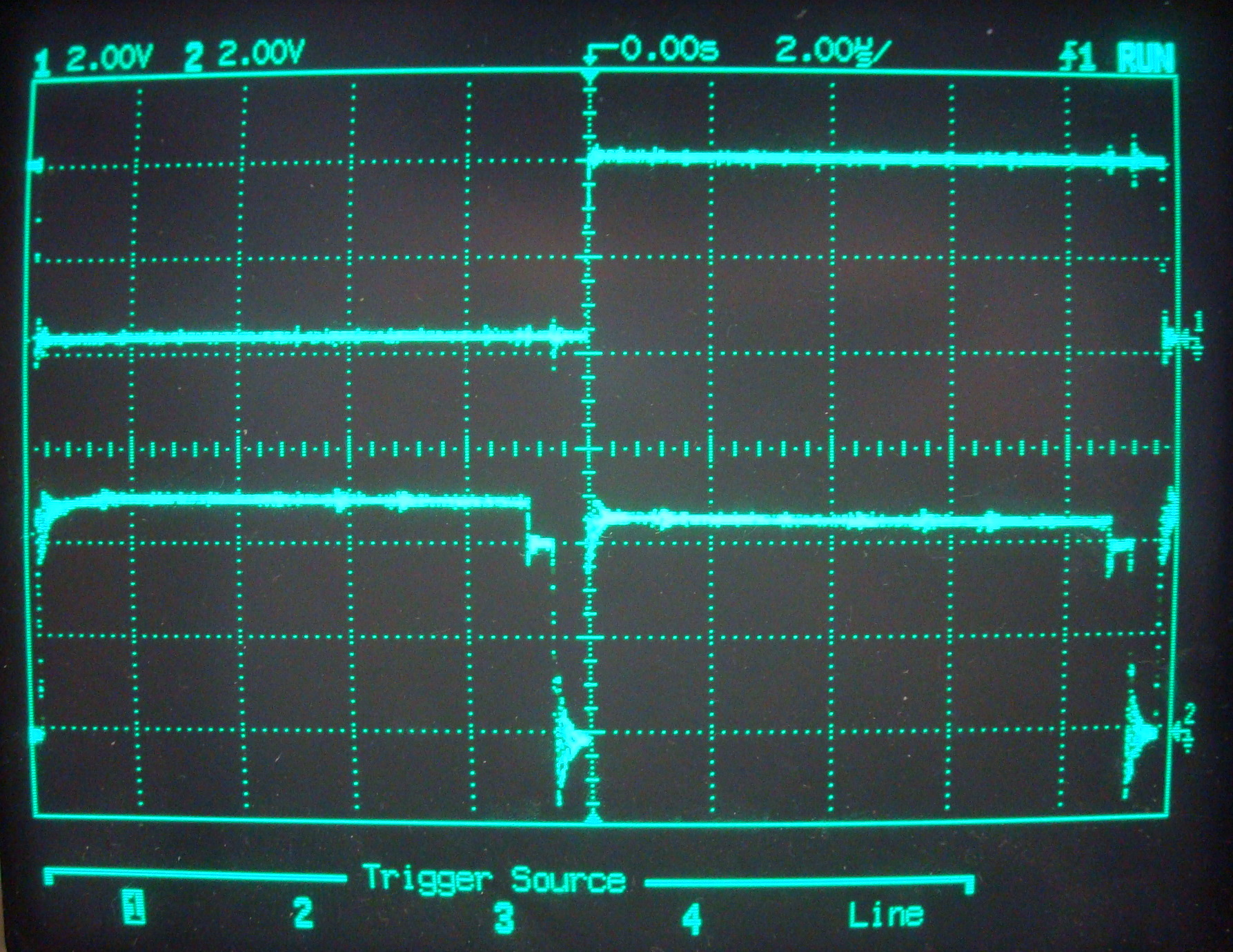
Now move your scope probes to the Q output of the flipflop, which shows the bit that is stored in the flipflop, and to the clock input of the 7474.
Verify that you see something like this:

In your report, explain which signal is which, and why this timing diagram is the correct one.
A software driver
A simple way to write a driver is to create two functions that can be called to set the LED ON, or to turn it OFF.
We can call the first function turnLEDOn, and the second one turnLEDOff.
Here is a way to organize your endless loop using these functions:
     LED        EQU        ????         ; enter the address energizing your Yi output

                ORG        0000
     loop:      jsr        turnLEDOn
                jsr        turnLEDOff
                jmp        loop

                ORG        0010
     turnLEDOn: ldaa       #1
                staa       LED
                rts

     turnLEDOff:ldaa       #0
                staa       LED
                rts
The JSR and RTS instructions are new. The JSR instruction jumps to a subroutine which is another name for function. It is like a jump except the processor also saves in the stack the address it must return to in the main program when it encounters the RTS instruction. RTS means return from subroutine, and it will pop off the stack the return address and put it in the Program Counter.
Assemble the above program by hand, and verify that you get a similar waveform as the last one you got before, where the time scale may have changed (why?).
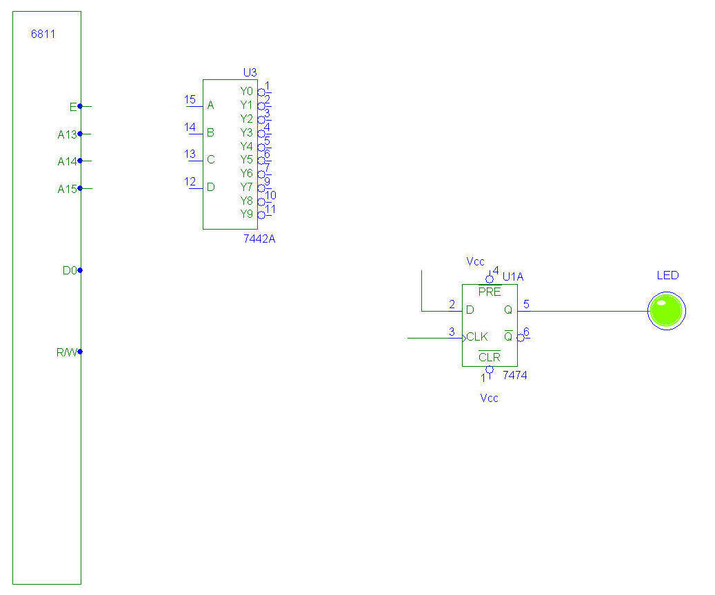
Schematics
You may use the figure below to create your full design.

