CSC270 Exercises on Memory-Mapped I/O
--D. Thiebaut 10:42, 4 April 2011 (EDT)
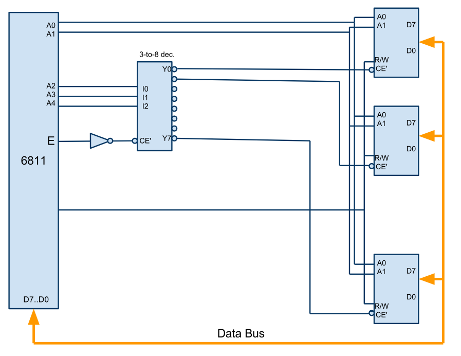
All the questions relate to the diagram below showing a simplified processor with 5 address lines, giving it a total address space of 2^5 = 32 bytes. This address space is "covered" by 8 memory chips, each containing 4 bytes.
- Question 1
- What is the timing diagram of a memory access cycle. Show the relationship of E, R/W, A4-A0, Yi, CE', and D7-D0.
- Question 2
- We want to sell a cheaper version of this computer, with on 4-byte RAM chip covering the low memory address ranges, and a 4-byte ROM chip covering the high address ranges. Redesign the system to match this new set of requirements.
- Question 3
- We want to sell a more expensive version of this computer, with 8 bytes of RAM and 4 bytes of ROM. The 8 bytes of RAM should be at consecutive memory addresses starting at 00h. We only have 4-byte RAM chips.
- Question 4
- Same as Question 3, but we now have available an 8-byte RAM chip. Redesign the system.
- Question 5
- Add a 1-bit register at an address not occupied by the RAM or the ROM, and wire it up as a write-only register whose output will be connected to an LED. We are in effect creating a 1-bit output port. Design such a system.
- Question 6
- Write a 6811 assembly program that stores 1, then 0, then 1, then 0, ad infinitum in the 1-bit port.
