Tutorial: Printed-Circuit Boards
--D. Thiebaut 12:37, 20 June 2011 (EDT)
This tutorial provides the series of steps required to go from schematics to a printed-circuit board (PCB) layout that can be sent away to a fabrication lab for manufacturing. The lab used in this tutorial is pcbexpress.com. The process illustrated below is certainly not that of an expert, but my recorded first attempt at generating a PCB layout from simple schematics. Feel free to edit or send comments and suggestions to thiebaut@cs.smith.edu . Many thanks to Paul Voss for showing me the whole process first and spending time going over each one in details.
Software
All are open-source.
- TinyCAD
- FreePCB
- ViewMate (get the free registration code via email to install)
- PCBExpress/Sunstone: Web site where to order PCB from.
Process
- First create schematics with TinyCAD
- Then route the lines on a 4-layer board with FreePCB
- Check the CAM files generated by FreePCB with ViewMate, and get a direct quote from PCBExpress.
An Example
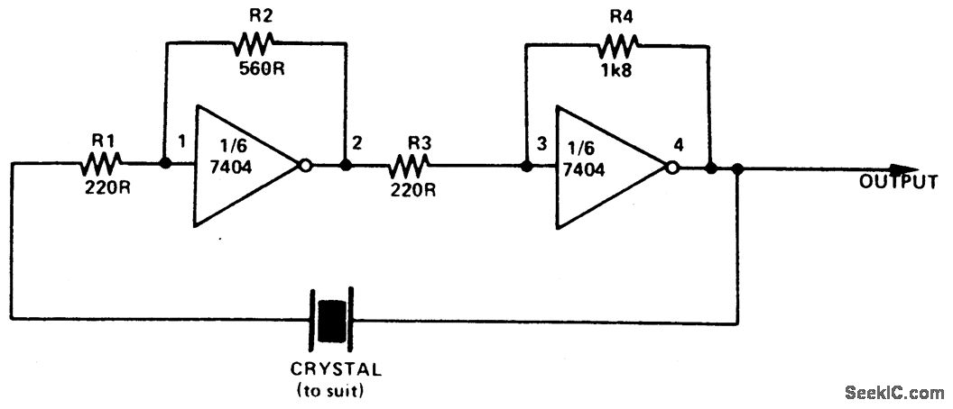
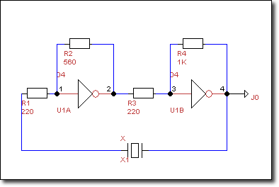
- We'll create a PCB for the following simple circuit taken from seekic.com:
TinyCAD
Generating the Schematics
- Open TinyCAD
- Open the 74TTL library in the left pane
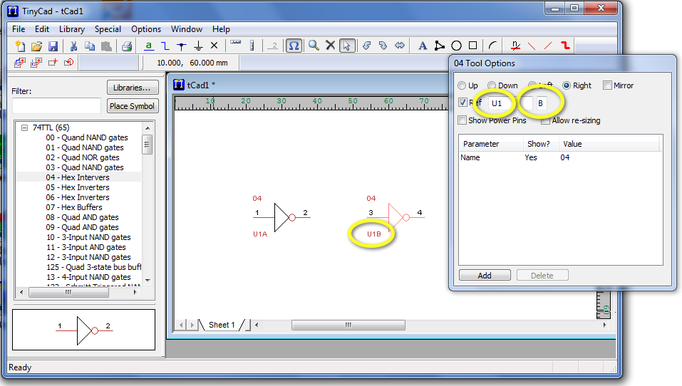
- Pick the Hex Inverters
- Drop two inverters on the blank schematics pane
- Update the reference for each gate (U1A and U1B) in the Tool Options window.
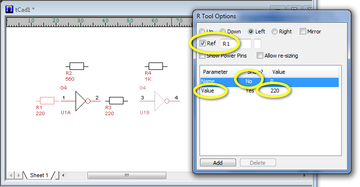
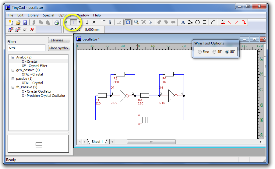
- Open the Analog library, and pick the Resistor, and drop it on the schematics pane where resistors are needed. Use the Tool Options window to set the orientation of the resistors to left.
- For each resistor, use the Tool Options menu to set the Ref to Rn where n is 1, 2, 3, or 4, and Add a value field to the Parameter list for indicating the value in ohm.
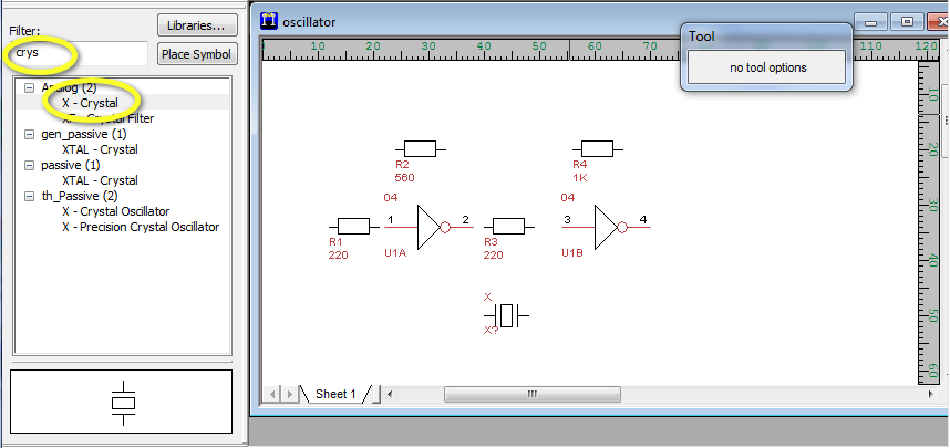
- To add the crystal, search for it in the Filter box and pick the X-Crystal symbol.
- It might be a good time to save your work!
- Click on the Wire tool button and use the mouse to connect all the component pins together, recreating the wiring of the original circuit.
- Add out output connector (J0 - Connection Output)
Assigning Packages to Parts
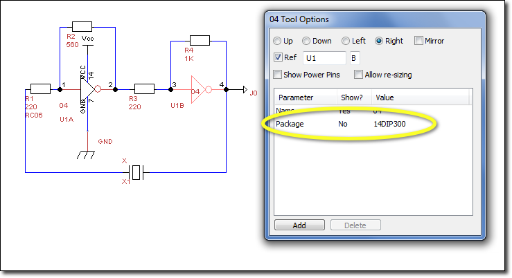
- Depending on the type of circuits you will be using, you can now edit your different parts and add a new Package field, as illustrated here for the 7404 chip.
- Refer to the FreePCB documentation for the type of packages supported. Here's the list of packages picked for this project:
U1   14DIP300
Rn   RC06
X1   CK12-B
J0   HOLE_100_SQR_200
- (where n in Rn is 1, 2, 3, and 4.)
- Assigning packages to the parts now will allow the FreePCB, our next software tool to automatically generate footprints for our parts.
Testing
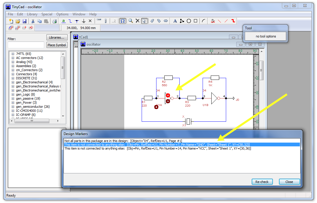
- Check your design by clicking on Special in the top menu, then Check Design Rules.
- Accept the defaults and click Check
- You should get a message indicating that Vcc and GND of the 7404 are not connected.
Generate the Net-List File
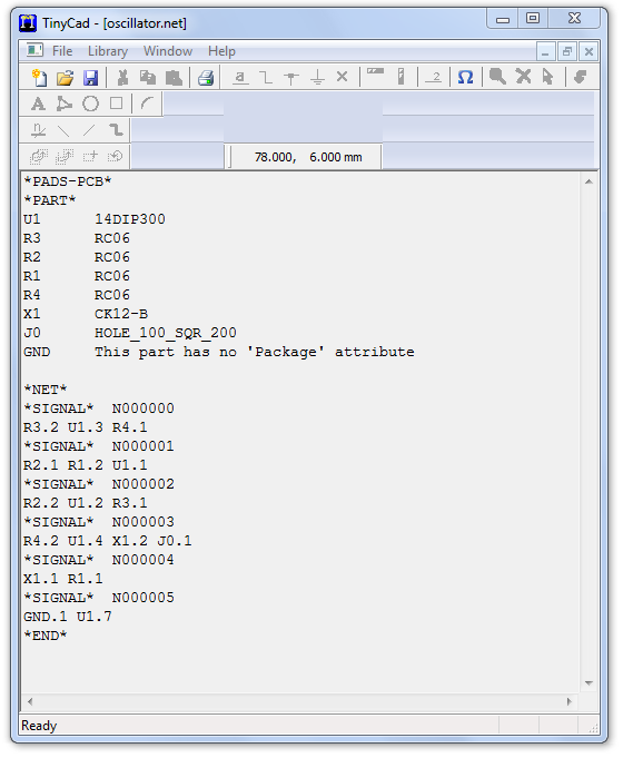
- Using the top menu, click Special, Create PCB Net List, select PADS-PCB for the format, and save to file.
- You should get the following output:
- You are now ready for the second step
FreePCB
- The official manual for FreePCB is a Must-Read and can be found here.
- Open FreePCB
- From the menu, File, New, and create a new project
- Name: oscillator
- Layers: 2 (sufficient for right now)
- accept all the other default value
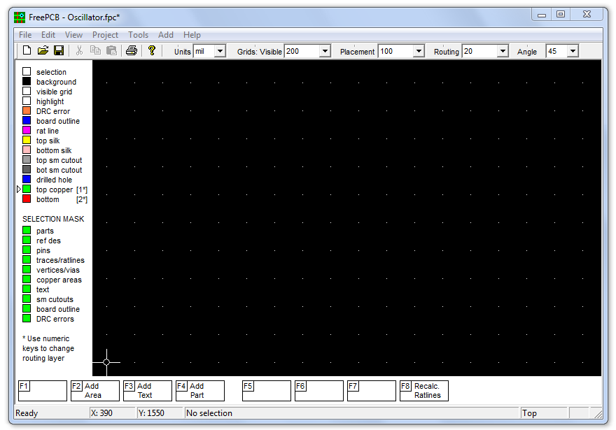
- Click Ok
- You should be presented with an empty grid:
Board Outline
- Create the outline of your board. This can be any polygone shape you can define by consecutive points.
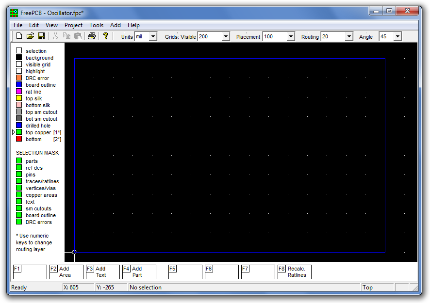
- From the top menu, click Add, Board Outline, then click points on the grid to create a rectangle. Don't worry about the size yet, all the points can be moved in or out later to create as tight a layout as you wish.
- Make sure your last point coincide with your first point.
Import the Net List file
- From the main menu, browse around your file system and pick the oscillator.net file created by TinyCAD in the steps above.
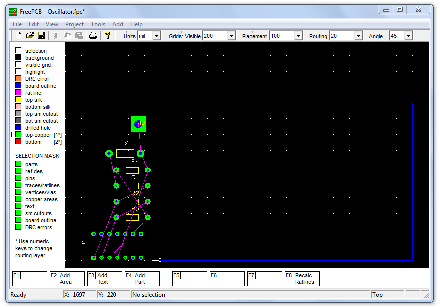
- FreePCB should show the parts and rat wires connecting the different parts of your circuit:
- Click on each part and use F4 (Move Part) to move the parts in a layout that minimizes rat lines crossings.
Adding New Elements
- Add two mounting holes for connecting the power to the board: from the menu select Add, Part, th_mounting_hole and pick two circular holes, making sure you give a reference to both of them (we use P1 and P2 here, for Power).
- Add the text "+5V" next to one of the just added mounting holes using the Add, Part, and Text menu options.
Converting Rat-Lines to Copper Traces
- For this project we selected only 2 different copper layers. We'll create traces on the top layer, and reserve the bottom layer for Ground.
- In the leftmost column, select the top copper [1*] so that the white arrow points to it.
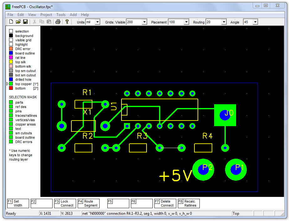
- Click on a rat-line, highlight it, and press the F4 key, or click on Route Segment to create a trace. The rat line disappears and is replaced by a green trace (top layer traces are green).
- Repeat the process until all the rat-lines have been replaced by traces, as illustrated below.
Adding Power Connections
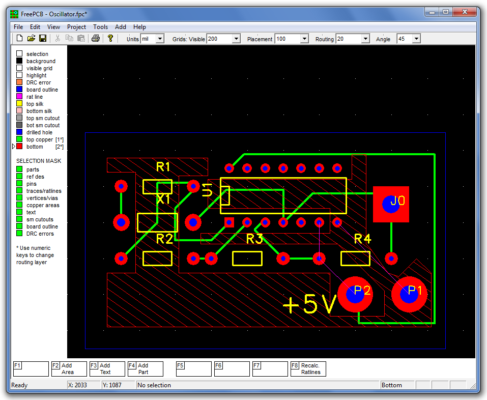
- We now add traces from the two Power Connecters to the 7404 power pins. For the +5V connection, we add a trace, and for Gnd, we use a copper area on the bottom copper layer.
- +5V
- Add, Net, pick a net name not already in used (e.g. N00000), then click on the Power Connector next to the +5V silk screen text, then click on Connect Pin; a rat line appears. Connect the rat line to Pin 14 (top-left) of the U1 circuit.
- GND
- Deselect the rat line, top silk, and top copper
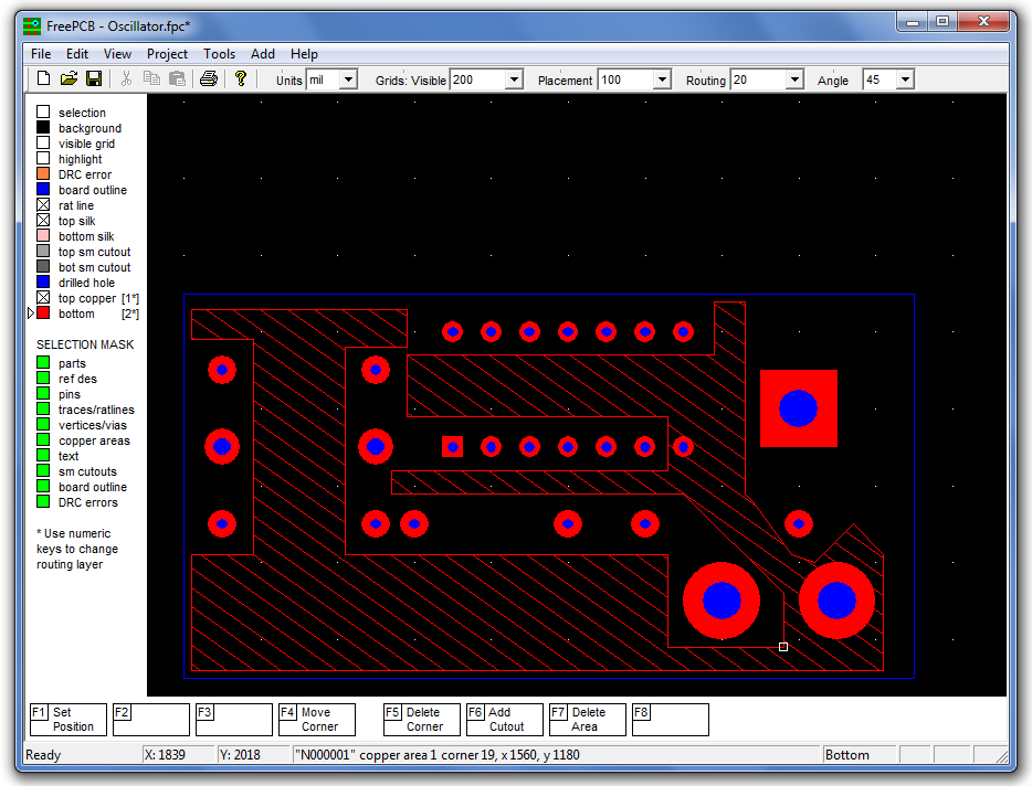
- Add, Copper Area, pick a net name not already in used (e.g. N00001), and bottom copper
- create a polygon that covers most of the board, and overlaps only Pin 7 of the 7404, and the GND connector.
Check the Design Rules
- It is possible that some areas or traces might be too close to other elements of the board. Check for possible problem areas by clicking Tools, Design Rules Check and select all default values offered.
- Problem areas will be indicated by red circles. Adjust the positioning and dimensions of your board through iterations until the Design Rules Check returns an empty report.
Create CAM Files
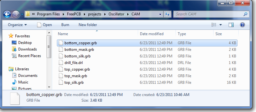
- Create the files that will be used to generate the PCB using the File, Generate CAM Files menu options.
- These files are available in this tgz archive file. (Note: remove the .data extension from the file before unzipping.)
ViewMate
- This step is to verify the design to ensure that it can be manufactured, and to order boards if necessary.
- Start PentaLogix's ViewMate DFM program
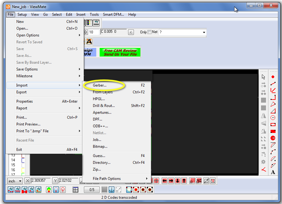
- Import the gerber files into the program: File, Import, gerber and select the CAM files that are very likely stored in the FreePCB project directory, under oscillator or whatever name you used for your project.
- You may get some warnings. Just click Continue to move on to the next step. If you get errors, then you'd better address them and go back to the previous steps of the design!
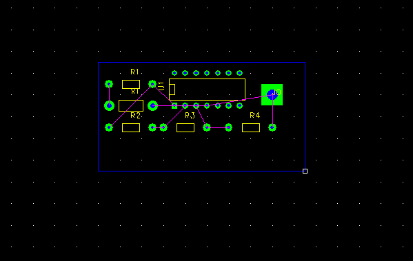
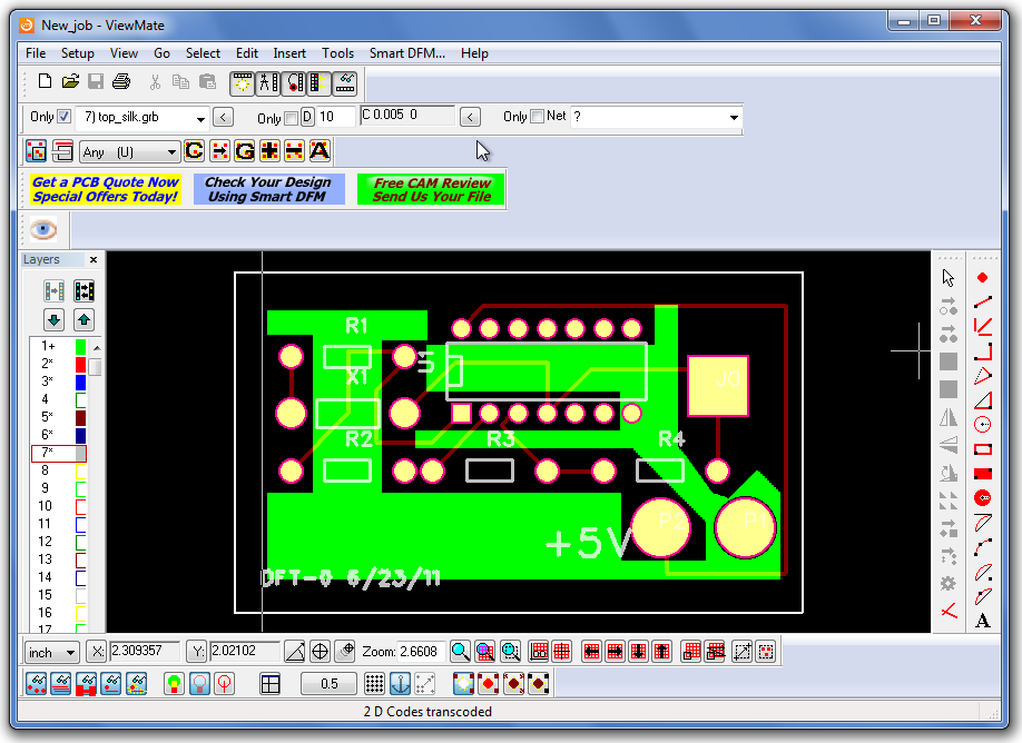
- You should recognize the PCB layout you created in the previous steps.
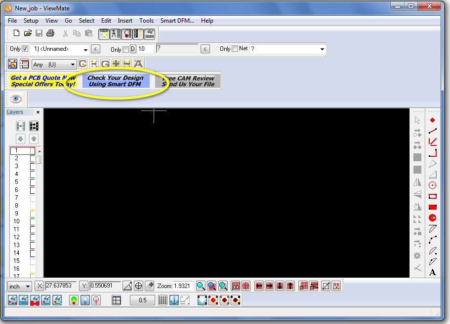
- Click on Check your Design using Smart DFM
- A new window opens up.
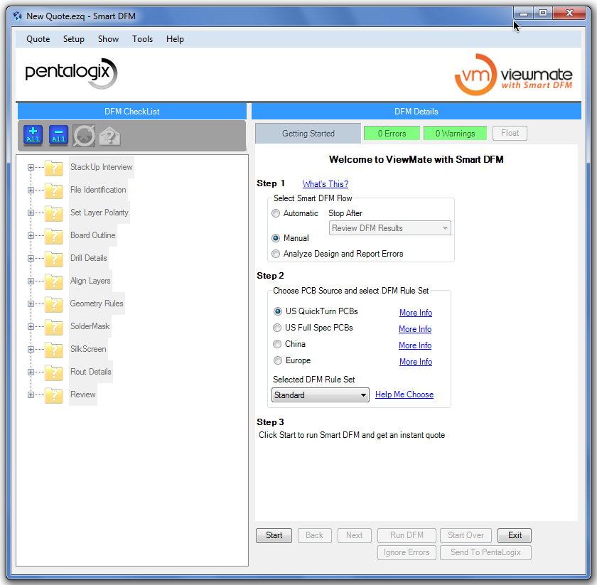
- Select Manual and US Quick Turn PCBs
- Click Start
- Select 2 Layer PCB Option, and keep the other default values
- Click Next
- Accept the board thickness offered as default
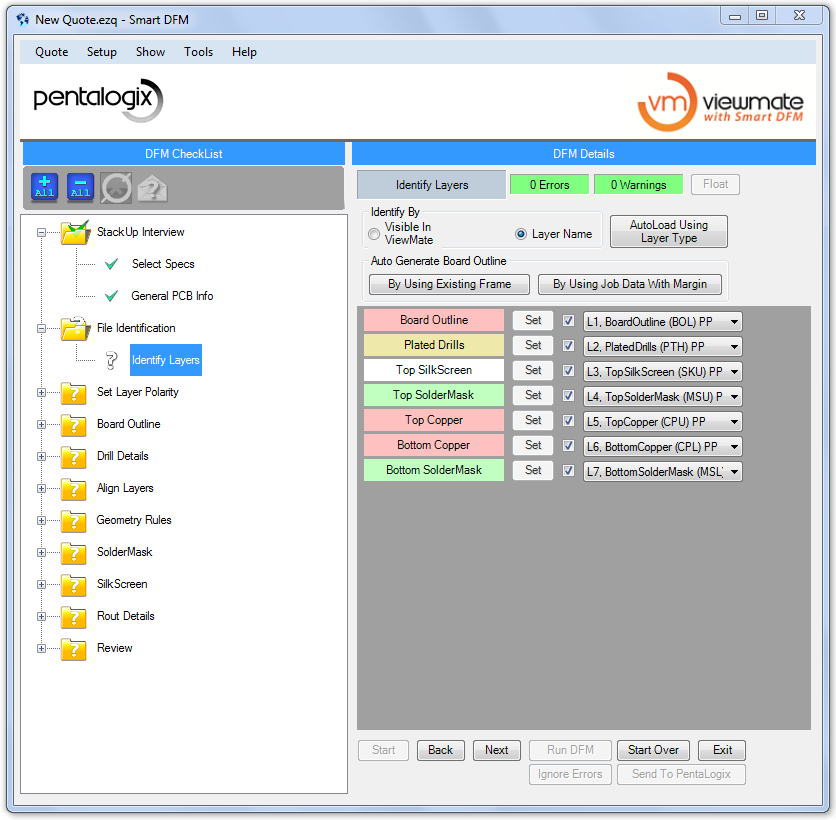
- Identify the different layers as shown below:
- Next
- Accept the Positive polarity for all the layers
- Next
- Verify that you do not have errors in your layout.
You should now be almost ready to order the board or boards from the form provided by PentaLogix. Happy soldering!
External Links
