Difference between revisions of "CSC270 Lab 4 2016"
(→XOR RS Flip-Flop) |
(→NOR RS Latch) |
||
| Line 11: | Line 11: | ||
<br /> | <br /> | ||
<br /> | <br /> | ||
| + | * Demonstrate the correct behavior of the circuit to your instructor. Show that the circuit "''remembers''" what switch is being activated. | ||
==NAND RS Latch== | ==NAND RS Latch== | ||
Revision as of 11:48, 16 February 2016
--D. Thiebaut (talk) 11:40, 16 February 2016 (EST)
Part 1
NOR RS Latch
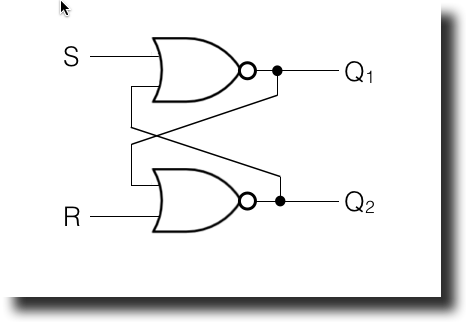
- Build an RS Latch with NOR gates (74LS02), as illustrated in the diagram below. Be careful, the pinout for the NOR gate is not the same as for the NAND gate.
- Energize the R and S inputs and transcribe the behavior of the Latch in a timing diagram.
- Demonstrate the correct behavior of the circuit to your instructor. Show that the circuit "remembers" what switch is being activated.
NAND RS Latch
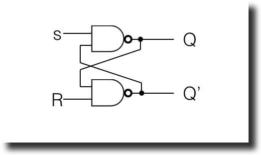
- Build an RS Latch with NAND gates, as illustrated below. Be careful, the pinout for the NOR gate is not the same as for the NAND gate, so you cannot just swap the two circuits.
- Energize the R and S inputs and transcribe the behavior of the Latch in a timing diagram.
Part 2
- Do the Tektronix Scope Lab
Part 3
- Capture the behavior of the NAND RS flipflop when both R and S are connected to the Test-Point 1 and Test-Point 2 of the HP test board. Make sure you connect the GND of the board to the GND of the kit.
- Capture the behavior of the NOR RS flipflop when both R and S are connected to the Test-Point 1 and Test-Point 2 of the HP test board. Same comment about the GND signals.
- Edit the capture you made (either draw it or edit the graphic file captured on your USB stick) and indicate which part of the timing diagram corresponds to the flipflop being
- in "memory" state,
- in "store 1" state,
- in "store 0" state, and
- in the "forbidden state."

