Difference between revisions of "CSC270 Class Page 2011"
(→Prof) |
(→Weekly Schedule) |
||
| Line 46: | Line 46: | ||
*** Truth tables | *** Truth tables | ||
*** Boolean functions | *** Boolean functions | ||
| − | * | + | *** canonical forms: the minterm canonical form |
| − | |||
| − | |||
| − | ** canonical forms: the minterm canonical form | ||
| − | |||
** examples of [http://klabs.org/history/ech/agc_schematics/index.htm schematics] from Nasa | ** examples of [http://klabs.org/history/ech/agc_schematics/index.htm schematics] from Nasa | ||
** logic gates | ** logic gates | ||
| Line 56: | Line 52: | ||
*** or gate (7432) | *** or gate (7432) | ||
*** not gate (7404) | *** not gate (7404) | ||
| + | ** <font color="magenta">'''Lab 1'''</font> | ||
| + | * '''Wednesday''': | ||
| + | [[Image:OrGateWithTransistors.gif|right]] | ||
| + | ** Some basic electricity concepts | ||
| + | ** Voltages, diagrams, Vcc, Gnd | ||
| + | ** Measuring voltages: different of potential ==> need two measuring points | ||
| + | ** Resistors | ||
| + | *** limit current | ||
| + | *** passive | ||
| + | *** property = resistance | ||
| + | *** unit of resistance = Ohm (Ω) | ||
| + | ** Ohm's Lay: V = RI | ||
| + | *** Apply law to simple circuits | ||
| + | *** Series and Parallel circuits with resistors | ||
| + | *** Exercises | ||
| + | ** How to generate a simple switch that generats ON/OFF, High/Low, 1/0 | ||
| + | ** The transistor | ||
| + | *** Emetter, Base, Collector | ||
| + | *** basic operations | ||
| + | *** simple circuit | ||
| + | ** Example of gates with transistors | ||
| + | ** Back to boolean functions | ||
| + | *** review of what is a min term. | ||
| + | *** Simplifying boolean functions | ||
* '''Friday''' | * '''Friday''' | ||
---- | ---- | ||
Revision as of 11:50, 26 January 2011
--D. Thiebaut 08:44, 7 January 2011 (EST)
Back to Main Page for CSC270
Contents
Prof
|
Dominique Thiébaut email |
Weekly Schedule
Back To Main Page
Links and Resources
Programs
- A Python program that generates a truth table.
Software
PSpice 9
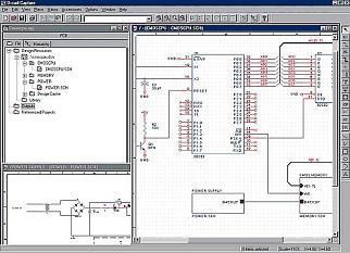
- Pspice 9, Student version. An nice alternative to drawing schematics by hand.
- This is a Windows version. (I have tried to make it work under wine/Mac OS X but haven't been able to make it load the libraries correctly)
- Make sure you select the schematics option when installing the software.
- Select Tools/Schematics when starting the editor
- The schematics editor is located in C:\Program Files\OrCAD_Demo\PSpice\PDesign.exe upon installation.
- Download here!
- PSpice Tutorial
Integrated Circuit Data-Sheets
- Java Applets demonstrating most logical gates
- Texas Instruments and Harris Semiconductors' Data Sheet Search Engine
- Fairchild Semiconductors' Data Sheet Search Engine
- 74LS00, 74LS01, 74LS02, 74LS03, 74LS04, 74LS05, 74LS08, 74LS09, 74LS10, 74LS12, 74LS13, 74LS15, 74LS20, 74LS21, 74LS22, 74LS26, 74LS27, 74LS28, 74LS30, 74LS32, 74LS33, 74LS37, 74LS38, 74LS40, 74LS42, 74LS47, 74LS48, 74LS51, 74LS54, 74LS55, 74LS74, 74LS75, 74LS76, 74LS83, 74LS85, 74LS86, 74LS90, 74LS95, 74LS138, 74HCT240, 74LS243, 74HCT244, 74LS259, 74HCT541
- 9368
- 2114 1Kx4 RAM ( with timing information )
- Octal D-Flipflop (we do not have these chips in our current collection of chips)
Motorola 68HC11 Documentation
- Good source of info on the 6811.
- 6811 FAQs.
- The official Motorola | 68HC11A8 Data Sheet. Fairly cryptic...
- A Motorola 6811 Manual. It is a nicely written refresher on many concepts of assembly language applied to the 6811.
- Check Section 3.2 on addressing modes (inherent, direct, extended, indexed, relative).
- Get a refresher for the different instruction types (arithmetic, shifts, control, etc) in Section 3.4.
- The condition code register is covered in Section 3.5.
- M68HC11 Technical Reference, Motorola
- Section 6.5 shows the instructions in logical groups.
- M68HC11 Pocket Reference.
- Very useful, on Page 15, a list of all the opcodes supported by the 6811, in numerical (hex) order.
- 68HC11A8 Technical Reference: a hardware and engineering description. of the 6811, its ports, and how it operates.
- See Section 10 for a cycle-by-cycle description of the execution of each instruction.
- See Appendix A, Figure A-14 for the timing diagram of a typical (multiplexed expansion) memory access.
Back To Main Page


