CSC270 Lab 4 2016
--D. Thiebaut (talk) 11:40, 16 February 2016 (EST)
This lab is the transition lab, from combinational logic, to sequential logic. The main instrument to observe sequential circuits is the oscilloscope, which you will be using for the first time today.
|
|
Part 1
NOR RS Latch
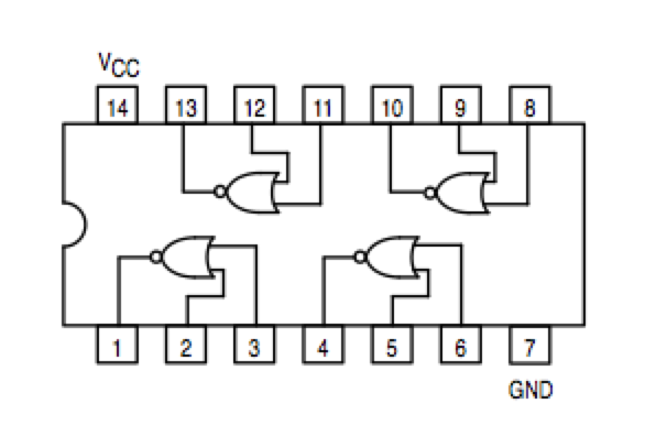
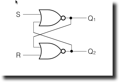
- Build an RS Latch with NOR gates (74LS02), as illustrated in the diagram below. Be careful, the pinout for the NOR gate is not the same as for the NAND gate.
- Energize the R and S inputs and transcribe the behavior of the Latch in a timing diagram.
- Demonstrate the correct behavior of the circuit to your instructor. Show that the circuit "remembers" what switch is being activated.
NAND RS Latch
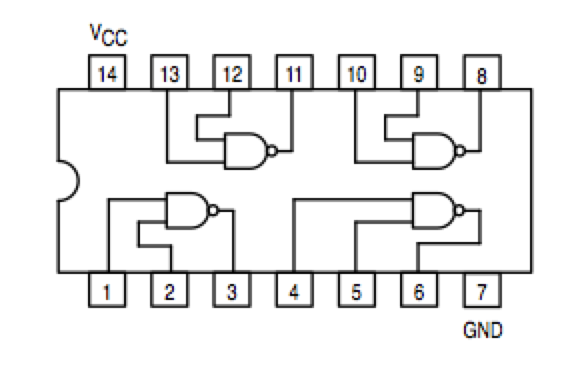
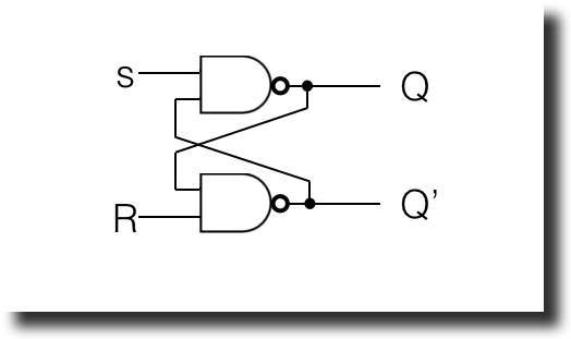
- Build an RS Latch with NAND gates, as illustrated below. Be careful, the pinout for the NOR gate is not the same as for the NAND gate, so you cannot just swap the two circuits.
- Energize the R and S inputs and transcribe the behavior of the Latch in a timing diagram.
- Demonstrate the correct behavior of the circuit to your instructor. Show that the circuit "remembers" what switch is being activated.
Part 2
|
Part 3
The digital kit has a clock signal that is oscillating at 1 KHz and 100 KHz. How accurate are these signals. Measure both of these signals and report on the error that might exist between the nominal value and what you measure. Is the error less than 1% of the nominal value? Less than 10% of the nominal value?
Part 4
- Capture the behavior of the NOR RS latch when both R and S are connected to the Test-Point 1 and Test-Point 2 of the HP test board. Make sure you connect the GND of the board to the GND of the kit.
- Edit the capture you made (either draw it or edit the graphic file captured on your USB stick) and indicate which part of the timing diagram corresponds to the latch being
- in "memory" state,
- in "store 1" state,
- in "store 0" state, and
- in the "forbidden state."
