Difference between revisions of "CSC270 Class Page 2009"

From dftwiki3
Jump to: navigation, search
(Weekly Schedule)
(Weekly Schedule)
Line 333: Line 333:
 
| Week 14 <br /> 4/27
 
| Week 14 <br /> 4/27
 
||  
 
||  
* '''Monday''': A bird's eye view of Computer Architecture.   
+
* '''Monday''': Selected Topics in Computer Architecture
** Processors: caches, pipeline, TLBs
+
<!--A bird's eye view of Computer Architecture.   
 +
** Processors: microprogram, caches, pipeline, Branch-Prediction Table
 
** Ports: USB
 
** Ports: USB
** Memory: dynamic RAM
+
** Memory: dynamic RAM-->
 
* '''Wednesday''':  
 
* '''Wednesday''':  
 
* <font color="purple">'''1-week Take-Home Final Exam'''</font>
 
* <font color="purple">'''1-week Take-Home Final Exam'''</font>

Revision as of 06:34, 20 April 2009

Back to Main Page for CSC270


Prof and TA

Dominique Thiébaut email
Dept. Computer Science
McConnell Hall, 208.
Telephone: 3854
Office hours MW 10:30-12:00, W 1-3, and by appointments


The TA for the class is Lei Lei, and her hours and location are available here

Weekly Schedule

Week Topics Reading
Week 1
1/26
  • Monday: Introduction to the semester
    • Syllabus
    • Overview of the class
    • combinational logic (1/4)
    • sequential logic( 1/4)
    • microprocessor logic (1/2)
    • Boolean Algebra
    • Truth tables
    • Boolean functions
  • Wednesday:
    • boolean functions
    • canonical forms: the minterm canonical form
    • exercises
    • examples of schematics from Nasa
    • logic gates
      • and gate (7408)
      • or gate (7432)
      • not gate (7404)

  • Binary numbers
  • Boolean algebra and Logic Gates
  • Basic theorems
  • Truth tables
  • Boolean functions
  • Canonical forms


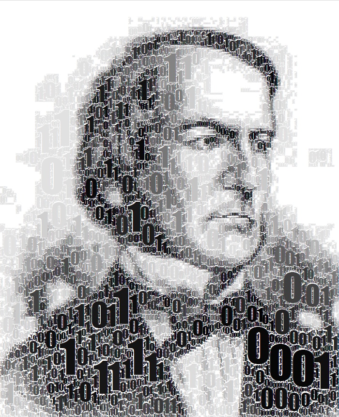
George Boole in zeros and ones
George Boole

Week 2
2/2
  • Monday
  • Wednesday
    • Python program to generate a truth table
    • A fully developed example: a majority voter, with 3 inputs, a Majority output, a Fault output, and two Id outputs identifying the faulty input.
    • Introduction to Karnaugh Maps

  • Canonical Forms
  • Universal gates: NAND and NOR
Week 3
2/9
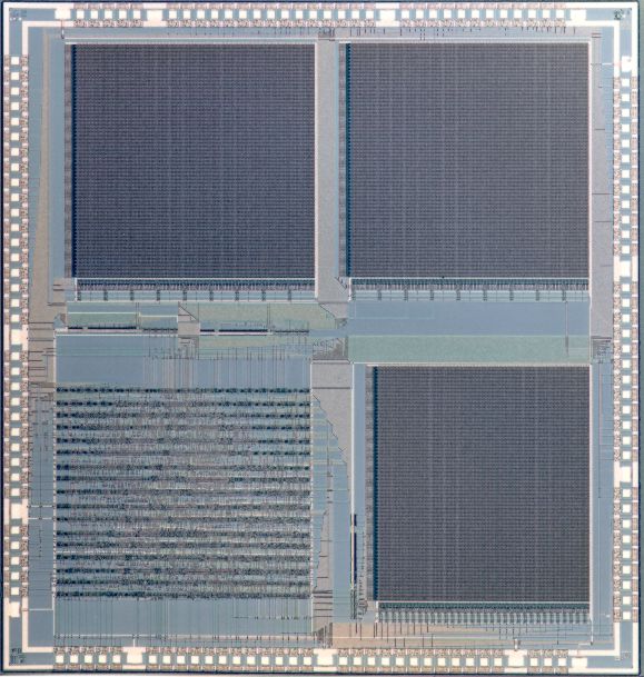
Die of a memory chip
  • Monday
    • Tips and Tricks: counting the number of inversions on a signal path
    • MSI: medium scale integration
      • decoders
      • active-low and active-high signals
      • The 74LS42 decoder
      • Animated 74154 decoder
      • Cascading decoders
      • multiplexers
      • Animated multiplexer
  • Wednesday
    • Do-it-yourself decoder: with/without enable, active-high/active-low signals
    • More decoder cascading
    • Multiplexers (mux)
    • Simplifying functions with multiplexers

  • Medium scale integration
  • The decoder
  • The multiplexer
  • Simplifying circuits with decoders or multiplexers


Week 4
2/16
  • Monday 2/16:
    • Timing diagrams and combinational circuits
    • the concepts of blocking and passing gates
    • Meeting the RS flip-flop
    • A single-input RS flip-flop
    • A single-input, pulsed RS flip-flop
    • The two-stage D flip-flop
    • understanding the D flip-flop
    • the 74LS74 datasheet
    • Exercises
  • 2/18 Rally Day, No Class

  •  
  • Sequential circuits
  • RS Flip-flop
  • D Flip-flop
Week 5
2/23
  • Monday
    • The D-flip-flop explained (Movie available on YouTube!)
    • A simple GYR sequencer
  • Wednesday
    • Continuation of the GYR sequencer
    • Let's not forget decoders!
    • Debouncing switches and clock signals
    • Python to the rescue! A program to simulate a sequencer
    • Exercises

  •  


Week 6
3/2
Calvin snow.jpg
CSC270 JKFlipflop.jpg
  • Monday: Snow Day
  • Wednesday:
    • Analysis: behavior of a 2-bit sequencer with equations D1 = Q1^Q0, D0=Q1'.
    • Random start, and forced reset
    • A GYR sequencer with an outside input signal.
    • Exercise
    • JK Flipflop


  • Sequencers with outside controls
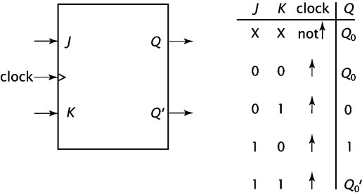
  • The JK flipflop
  • Building sequencers with JK flipflops
Week 7
3/9
  • 3/11 Midterm Exam
  • Midterm Preparation (Note that in Question 5 the Inputs should be labeled I0, I1, and I2. 0 is connected to I2, which is the MSB)

  •  
  •  


Week 8
3/16
DancingCalving.gif


Week 9
3/23
6811Motorola.jpg
  • Monday:
    • The 6811 Processor: references
      • The official Motorola 68HC11A8 Data Sheet. Fairly cryptic...
      • A Motorola 6811 Manual. It is a nicely written refresher on many concepts of assembly language applied to the 6811.
        • Check Section 3.2 on addressing modes (inherent, direct, extended, indexed, relative).
        • Get a refresher for the different instruction types (arithmetic, shifts, control, etc) in Section 3.4.
        • The condition code register is covered in Section 3.5. Skip Section 4.
      • M68HC11 Technical Reference, from Motorola.
        • Section 6.5 shows the instructions in logical groups.
    • M68HC11 Pocket Reference.
      • Very useful, on Page 15, a list of all the opcodes supported by the 6811, in numerical (hex) order.
    • 68HC11A8 Technical Reference: a hardware & engineering description. of the 6811, its ports, and how it operates.
        • See Section 10 for a cycle-by-cycle description of the execution of each instruction.
        • See Appendix A, Figure A-14 for the timing diagram of a typical (multiplexed expansion) memory access.
    • 6811 Instruction Set, with hexadecimal opcodes. A reverse map, from hex to instructions can be found here.
    • 2-Page List of all the 6811 Instructions
    • Software for the 6811
  • Wednesday:
    • Concentration on Assembly Language
    • CSC270 6811 Listing Format.png
      Listing format
      • opcodes, mnemonics, directives, columnar format
    • The instructions
    • Addressing Modes: inherent, immediate, direct, extended, indexed, relative
    • Exercises, exercises, exercises!!!


Week 10
3/30
  • Monday:
    • Quiz on the information in 6811 Manual (You can skip Section 4)
    • Timing Diagrams: conventions (transitions, floating signals, unknown, propagation times)
    • The E and R/W' signals (see the Google book MC68HC11, an introduction by Han-Way Huang, Section 5.7)
    • The timing of the execution of a 6811 instruction
    • the E signal
    • the R/W' signal
    • Timing of complete instructions
      • LDAA #3
      • LDAA 03
      • LDAA 0003
      • LDAA 3,X
      • STAA 03
      • STAA 0003
      • STAA 3,X
    • Timing of a full program
  • Wednesday
    • Exercise: timing of an endless loop (preparation for the lab)
    • The conditional branch instructions and relative addressing mode

  •  
Week 11
4/6
  • Monday
    • Relative Addressing
    • BRA, BEQ, BNE, etc.
    • Exercises
  • Wednesday
    • Designing a 1-bit I/O output port.
    • Decoding the address bus
      • Ideal case: 1 RAM chip
      • Case 2: 1 RAM + 1 ROM chips covering the whole space
      • Case 3: 1 RAM + 1 ROM chips covering only 1/4 each of the whole address space
      • Case 4: Add a memory-mapped 1-bit ouput port in the unused space

  •  


Week 12
4/13
CSC270 74244.png
CSC270 74541.png
CSC270 74240.png
  • Monday:
  • Wednesday
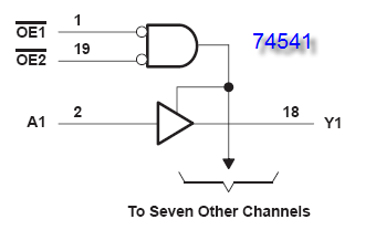
    • Tri-state drivers

  • Read the section on Tri-state buffers in Mano's textbook
Week 13
4/20
CSC270 centronics.jpg
CSC270 parallelPortTiming.jpg
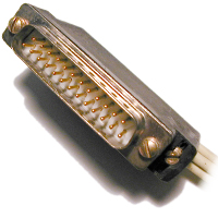
  • Monday: The Parallel Port. Control, Status, Data registers.
    • Signals (see this link)
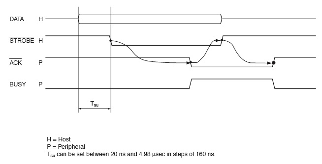
    • Protocol with Strobe and Ack (see this document)
    • Driver code for outputting a byte to a Centronics Port
  • Wednesday: the 2114 RAM
    • Timing requirement of the 2114
    • Wiring a 2114 to a 6811
    • Software testing

Week 14
4/27
  • Monday: Selected Topics in Computer Architecture
  • Wednesday:
  • 1-week Take-Home Final Exam
  • No lab

  •  
  •  


Back To Main Page


Links and Resources

Programs

Software

Pspice9.jpg

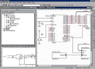
PSpice 9

  • Pspice 9, Student version. An nice alternative to drawing schematics by hand.
  • This is a Windows version. (I have tried to make it work under wine/Mac OS X but haven't been able to make it load the libraries correctly)
  • Make sure you select the schematics option when installing the software.
  • Select Tools/Schematics when starting the editor
  • The schematics editor is located in C:\Program Files\OrCAD_Demo\PSpice\PDesign.exe upon installation.
  • Download here!
  • PSpice Tutorial

Integrated Circuit Data-Sheets

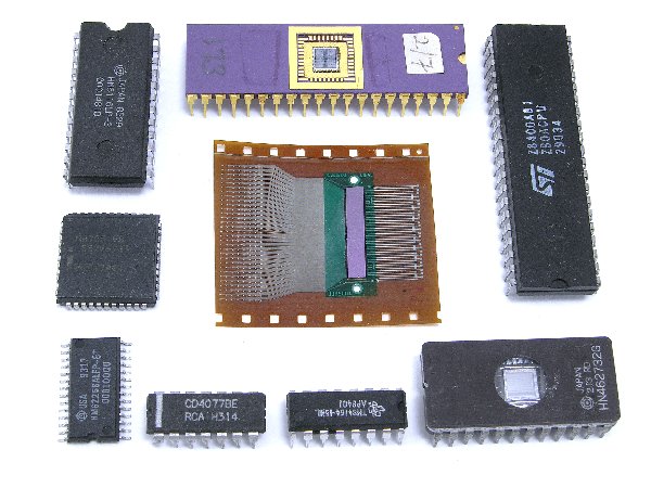
Ic.jpg

Motorola 68HC11 Documentation

6811.jpg
  • Good source of info on the 6811.
  • 6811 FAQs.
  • The official Motorola | 68HC11A8 Data Sheet. Fairly cryptic...
  • A Motorola 6811 Manual. It is a nicely written refresher on many concepts of assembly language applied to the 6811.
    • Check Section 3.2 on addressing modes (inherent, direct, extended, indexed, relative).
    • Get a refresher for the different instruction types (arithmetic, shifts, control, etc) in Section 3.4.
    • The condition code register is covered in Section 3.5.
  • M68HC11 Technical Reference, Motorola
    • Section 6.5 shows the instructions in logical groups.
  • M68HC11 Pocket Reference.
    • Very useful, on Page 15, a list of all the opcodes supported by the 6811, in numerical (hex) order.
  • 68HC11A8 Technical Reference: a hardware and engineering description. of the 6811, its ports, and how it operates.
    • See Section 10 for a cycle-by-cycle description of the execution of each instruction.
    • See Appendix A, Figure A-14 for the timing diagram of a typical (multiplexed expansion) memory access.


Back To Main Page