Difference between revisions of "CSC270 Class Page 2011"
(→Weekly Schedule) |
(→Programs) |
||
| (144 intermediate revisions by the same user not shown) | |||
| Line 20: | Line 20: | ||
Ford Hall, 356.<br /> | Ford Hall, 356.<br /> | ||
Telephone: 3854<br /> | Telephone: 3854<br /> | ||
| − | Office | + | Office Hours: M:4-5, T3-4, W3-4, and by appointment |
|} | |} | ||
| Line 26: | Line 26: | ||
=Weekly Schedule= | =Weekly Schedule= | ||
| − | + | ==First 1/2 of Semester== | |
| + | |||
{| style="width:100%" border="1" | {| style="width:100%" border="1" | ||
|- style="background:#ffdead;" | |- style="background:#ffdead;" | ||
| Line 46: | Line 47: | ||
*** Truth tables | *** Truth tables | ||
*** Boolean functions | *** Boolean functions | ||
| − | * | + | *** canonical forms: the minterm canonical form |
| − | |||
| − | |||
| − | ** canonical forms: the minterm canonical form | ||
| − | |||
** examples of [http://klabs.org/history/ech/agc_schematics/index.htm schematics] from Nasa | ** examples of [http://klabs.org/history/ech/agc_schematics/index.htm schematics] from Nasa | ||
** logic gates | ** logic gates | ||
| Line 56: | Line 53: | ||
*** or gate (7432) | *** or gate (7432) | ||
*** not gate (7404) | *** not gate (7404) | ||
| + | ** <font color="magenta">'''Lab 1'''</font> | ||
| + | * '''Wednesday''': | ||
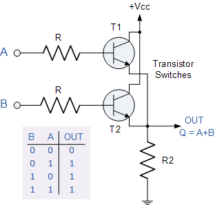
| + | [[Image:OrGateWithTransistors.gif|200px|right]] | ||
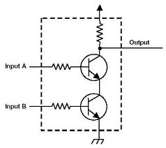
| + | [[Image:AndGateWithTransistors.jpg|200px|right]] | ||
| + | ** Some basic electricity concepts | ||
| + | ** Voltages, diagrams, Vcc, Gnd | ||
| + | ** Measuring voltages: different of potential ==> need two measuring points | ||
| + | ** Resistors | ||
| + | *** limit current | ||
| + | *** passive | ||
| + | *** property = resistance | ||
| + | *** unit of resistance = Ohm (Ω) | ||
| + | ** Ohm's Lay: V = RI | ||
| + | *** Apply law to simple circuits | ||
| + | *** Series and Parallel circuits with resistors | ||
| + | *** Exercises | ||
| + | ** How to generate a simple switch that generats ON/OFF, High/Low, 1/0 | ||
| + | ** The transistor | ||
| + | *** Emetter, Base, Collector | ||
| + | *** basic operations | ||
| + | *** simple circuit | ||
* '''Friday''' | * '''Friday''' | ||
| + | ** Example of gates with transistors | ||
| + | ** Back to boolean functions | ||
| + | *** [[CSC270 Exercise: Duality | Exercise]] | ||
| + | *** review of what is a minterm. | ||
| + | *** Simplifying boolean functions | ||
| + | *** Maxterms | ||
---- | ---- | ||
| − | * [[CSC270_Lab_1 | Lab #1 ]] | + | * [[CSC270_Lab_1 | Lab #1 ]]. (Good [[CSC270 Tips and Good Examples for writing a lab report|example]] of a lab report]]) |
| − | + | * [[CSC270 Homework 1 2011 | Homework #1]] | |
|| | || | ||
* Binary numbers | * Binary numbers | ||
| Line 75: | Line 99: | ||
|| | || | ||
* '''Monday''' | * '''Monday''' | ||
| + | [[Image:Calvin snow.jpg|150px|right]] | ||
** lecture | ** lecture | ||
| + | *** What is a switch? i.e. how does a switch from the HeathKit generate a high or low voltage? | ||
| + | *** We are programmers! Verifying circuits with simple [[CSC270 GenerateTruthTable.py|programs]]! | ||
| + | *** The binary adder. 2-bit, and 3-bit versions | ||
| + | *** the NAND and NOR gates: universal gates | ||
** lab | ** lab | ||
| + | *** [[CSC270_Lab_2 | Lab #2 ]] | ||
* '''Wednesday''' | * '''Wednesday''' | ||
| + | ** Snow Day! | ||
* '''Friday''': No Class | * '''Friday''': No Class | ||
---- | ---- | ||
| − | * | + | * [[CSC270_Lab_2 | Lab #2 ]] |
| + | * [[CSC270 Homework 2 2011 | Homework #2]] | ||
|| | || | ||
* | * | ||
| Line 87: | Line 119: | ||
| Week 3 <br /> 2/7 | | Week 3 <br /> 2/7 | ||
|| | || | ||
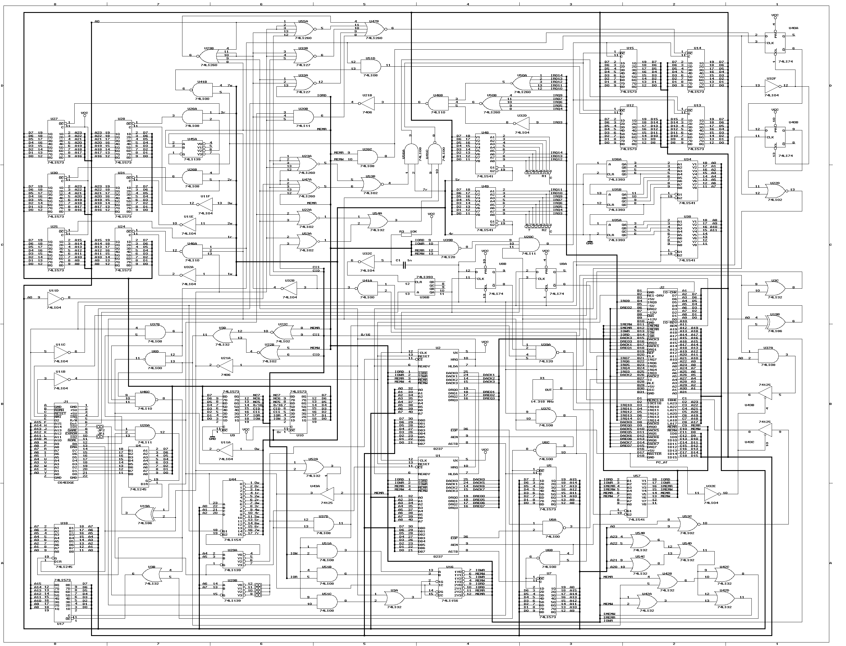
| + | [[Image:PCSchematics.gif|250px|right]] | ||
* '''Monday''' | * '''Monday''' | ||
** lecture | ** lecture | ||
| − | ** | + | *** Schematics and logic gates |
| + | *** Karnaugh Maps | ||
| + | *** Nand/Nor circuits | ||
| + | *** Decoder | ||
| + | *** [[CSC270 Exercises: Karnaugh Maps, Nands, Nors | Exercises on Karnaugh maps, nands, and majority voters]] | ||
| + | ** [[ CSC270 Lab 3 2011| Lab #3]] | ||
* '''Wednesday''' | * '''Wednesday''' | ||
| + | ** Lecture | ||
| + | *** Don't Care conditions in Karnaugh Maps | ||
| + | *** Decoders | ||
| + | ** Continuation of [[ CSC270 Lab 3 2011| Lab #3]] | ||
* '''Friday''': No Class | * '''Friday''': No Class | ||
---- | ---- | ||
| − | * | + | * [[ CSC270 Lab 3 2011 | Lab #3]] |
| + | * [[CSC270 Homework 3 2011 | Homework #3]] | ||
|| | || | ||
| − | * | + | * Karnaugh maps are covered in Chapter 3. |
| + | * Decoders are covered in Chapter 4. | ||
<!-- ================================================================== --> | <!-- ================================================================== --> | ||
|- style="background:#eeeeff" valign="top" | |- style="background:#eeeeff" valign="top" | ||
| Line 102: | Line 146: | ||
* '''Monday''' | * '''Monday''' | ||
** lecture | ** lecture | ||
| − | ** | + | *** another way to draw NANDs and NORs... |
| + | *** relationship between<br /><br /><tt> if ( a==b ) { ... }</tt><br /><br />and logic gates | ||
| + | *** active-low/active-high signals and circuits | ||
| + | *** decoders with active-low outputs: most common! | ||
| + | *** '''Exercise''': Implement f = Σ(1,3,4,5) with a decoder with '''active-high''' outputs | ||
| + | *** '''Exercise''': Implement f = Σ(1,3,4,5) with a decoder with '''active-low''' outputs | ||
| + | *** decoders with an enable input | ||
| + | *** cascading decoders | ||
| + | *** designing a 3-to-8 decoder with the 4-to-10 7442 decoder | ||
| + | ** [[ CSC270 Lab 4 2011 | Lab #4]] | ||
* '''Wednesday''' | * '''Wednesday''' | ||
| + | ** The Multiplexer circuit | ||
| + | ** The RS flipflop | ||
* '''Friday''' | * '''Friday''' | ||
| + | ** Catch-up day | ||
---- | ---- | ||
| − | * | + | * [[ CSC270 Lab 4 2011 | Lab #4]] |
| + | * [[CSC270 Homework 4 2011 | Homework #4]] and [[CSC270 Homework 4 Solution 2011|Solution]] | ||
|| | || | ||
* | * | ||
| Line 114: | Line 171: | ||
|| | || | ||
* '''Monday''' | * '''Monday''' | ||
| + | [[Image:BoardCapture1.jpg|100px|right]] | ||
| + | [[Image:BoardCapture2.jpg|100px|right]] | ||
| + | [[Image:BoardCapture3.jpg|100px|right]] | ||
** lecture | ** lecture | ||
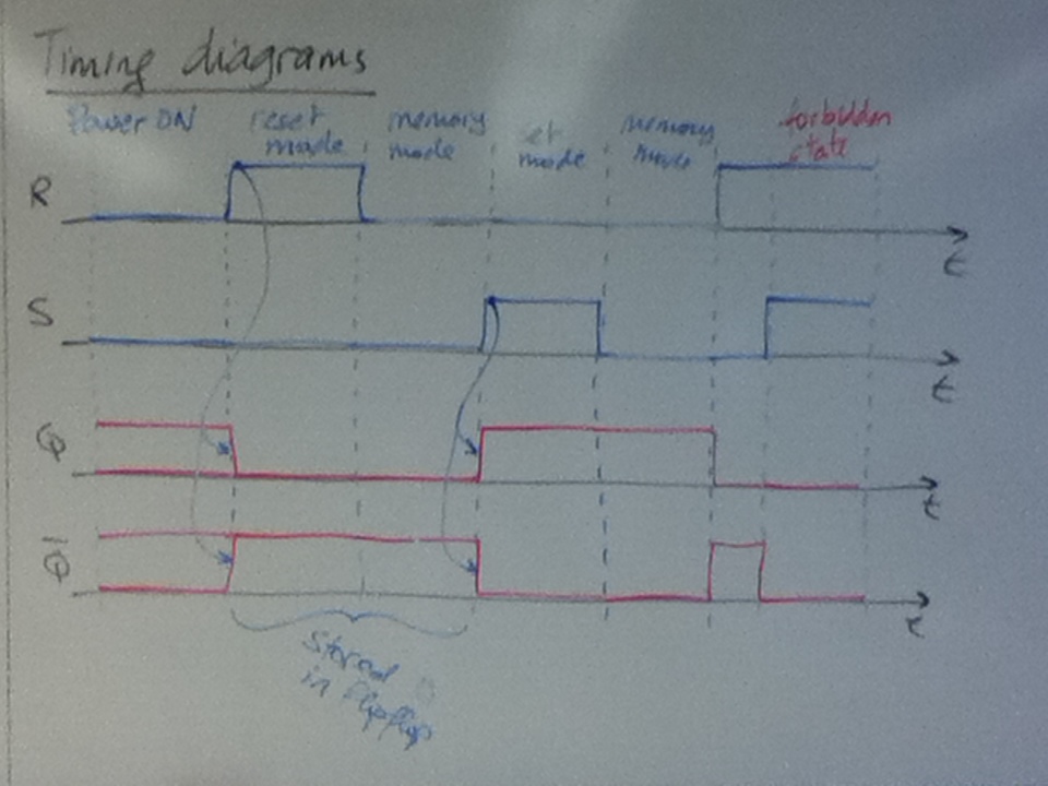
| − | ** | + | *** the RS Flipflop |
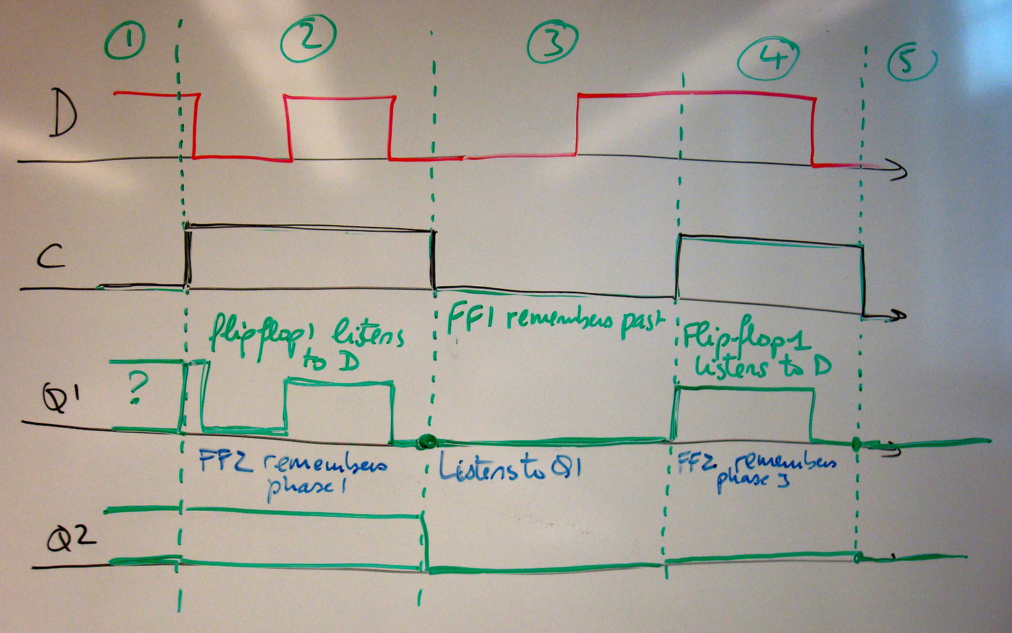
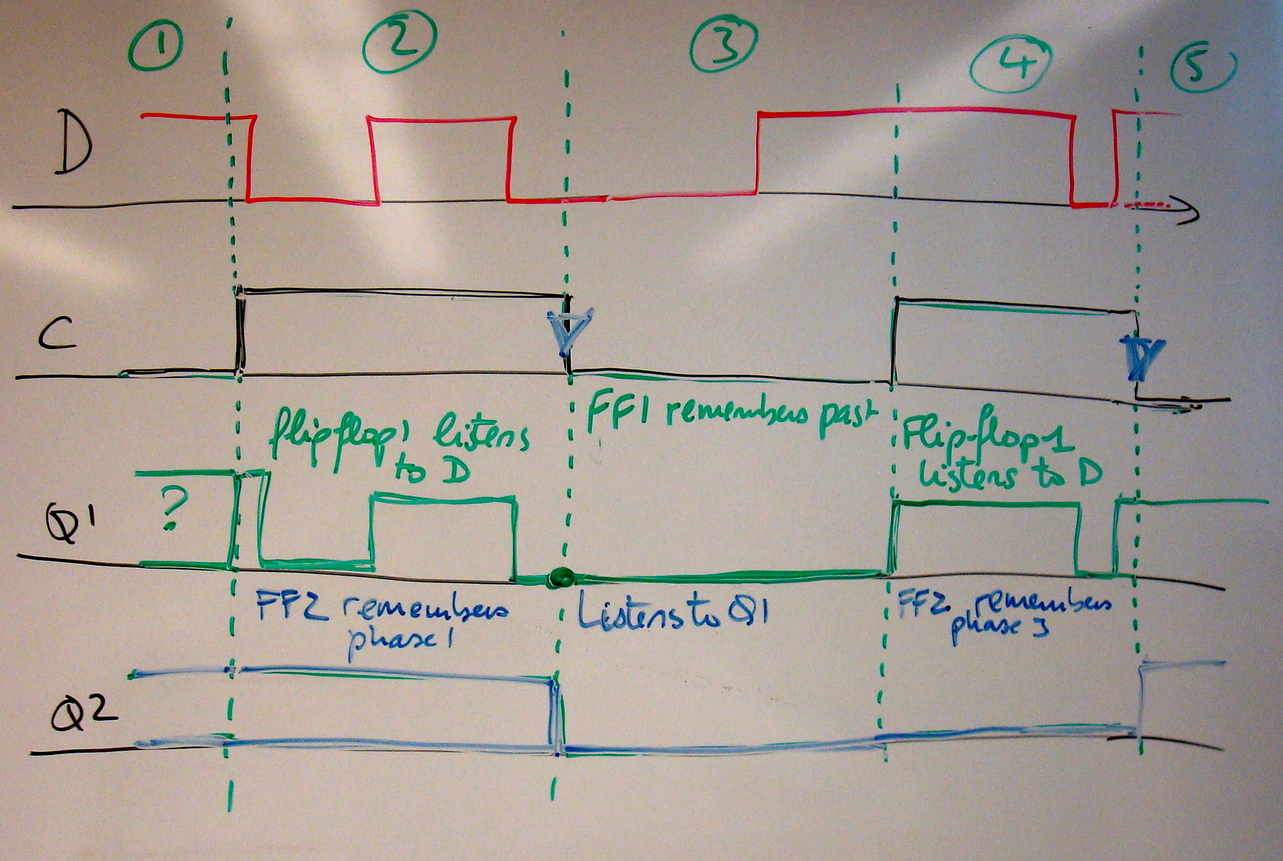
| + | *** Timing Diagrams | ||
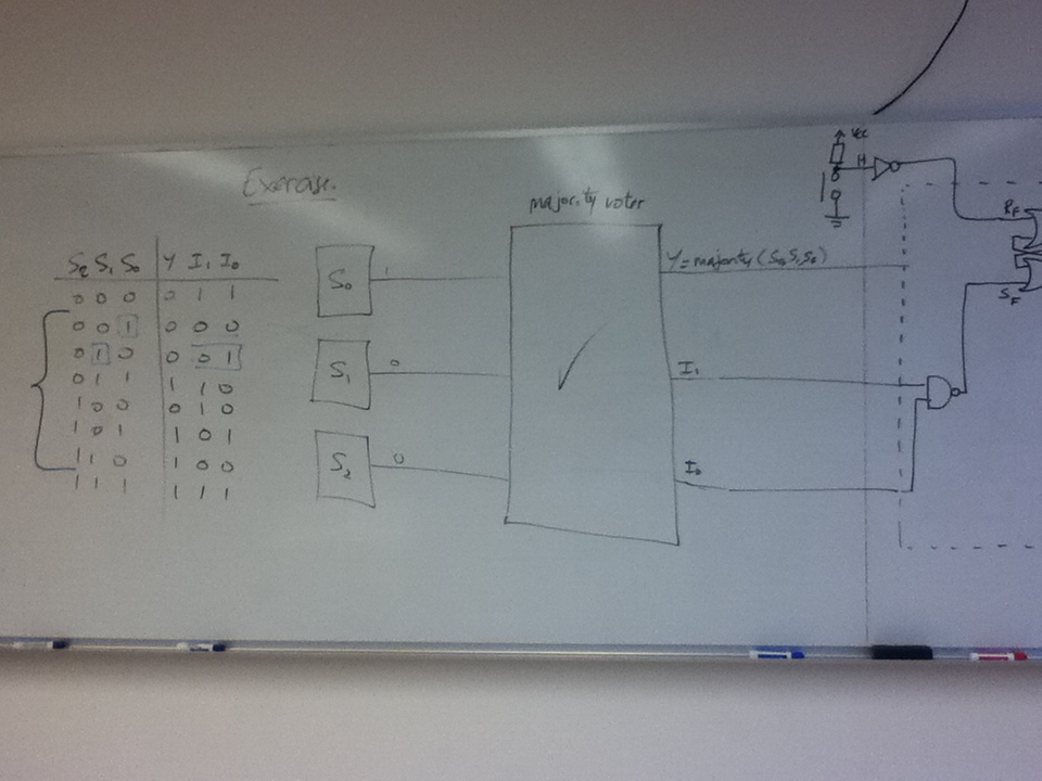
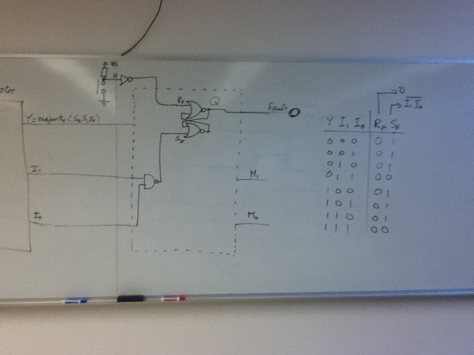
| + | *** '''Exercise''': | ||
| + | ::::''Design a majority voter that remembers when a fault occurs. First design a simple one that keeps track of the fact that a fault occurred in the past. Add a reset button to reset the fault signal. Then modify your design so that the majority voter not only remembers that there was a fault, it also remembers the Id of the faulty device.'' | ||
| + | *** The oscilloscope | ||
| + | **** Sampling | ||
| + | **** Periodic signals | ||
| + | **** Frequence | ||
| + | **** Peak-to-peak voltages | ||
| + | **** Trigger: Rule = always trigger on the slower of two signals! | ||
| + | ** [[CSC270 Lab 5 2011| Lab #5]] | ||
* '''Wednesday''': <font color="magenta">'''Rally Day'''</font> | * '''Wednesday''': <font color="magenta">'''Rally Day'''</font> | ||
* '''Friday''' | * '''Friday''' | ||
| + | [[Image:DFlipFlop_board1.jpg|100px|right]] | ||
| + | [[Image:DFlipFlop_board2.jpg|100px|right]] | ||
| + | [[Image:DFlipFlop_board3.jpg|100px|right]] | ||
| + | ** The RS Flip-flop: review | ||
| + | ** Making it work with a ''clock'' signal | ||
| + | ** Ideally we need a ''pulse'' to ''latch'' information in the flip-flop | ||
| + | ** Latching on the Low-to-High transition of the ''clock'' | ||
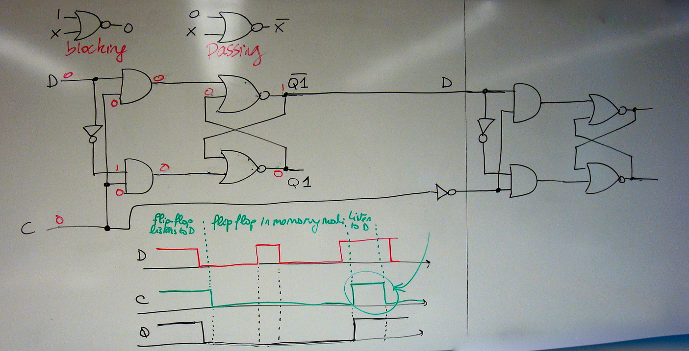
| + | ** the D Flip-flop: two RS flip-flops working in ping-pong mode | ||
| + | ** The [http://cs.smith.edu/~thiebaut/classes/270/datasheets/sn74ls74arev5.pdf 74LS74] circuit. | ||
| + | ** Timing diagram of a D Flip-flop | ||
| + | ** <font color="magenta">'''Mini Lab 1'''</font>: wire up a 7474 and observe its behavior. | ||
| + | |||
---- | ---- | ||
| − | * | + | * [[CSC270 Lab 5 2011| Lab #5]] |
| + | * [[CSC270 Homework 5 2011 | Homework #5]] | ||
|| | || | ||
| − | * | + | * The D-Flip-flop is covered in Section 5.3 of Mano. |
<!-- ================================================================== --> | <!-- ================================================================== --> | ||
|- style="background:#eeeeff" valign="top" | |- style="background:#eeeeff" valign="top" | ||
| Line 128: | Line 211: | ||
* '''Monday''' | * '''Monday''' | ||
** lecture | ** lecture | ||
| − | ** | + | *** Low-to-high and High-to-low clock inputs |
| + | *** A first 2-state state-machine with a D-Flip-flop | ||
| + | *** Duty cycle of a signal = %age of time ON / Period | ||
| + | *** The Moore Model, or Moore Machine | ||
| + | *** How do we find a way to generate this machine? | ||
| + | *** Characteristic Table of the D-Flip-flop | ||
| + | *** State diagram | ||
| + | *** State table | ||
| + | *** Activation table | ||
| + | ** [[CSC270 Lab 6 2011 | Lab]] | ||
| + | *** [[CSC270 Lab 6 2011 | Lab #6]] | ||
* '''Wednesday''' | * '''Wednesday''' | ||
| + | ** [[CSC270 Exercises on FSM| Exercises on FSM]] | ||
* '''Friday''' | * '''Friday''' | ||
---- | ---- | ||
| − | * | + | * [[CSC270 Lab 6 2011 | Lab #6]] |
| + | |||
|| | || | ||
| − | * | + | * Read Chapter 5 |
| + | * The chapter introduces several flip-flops. We'll look at the JK briefly in class. The chapter also introduces two different approaches to designing finite state machines: the Moore machine and the Mealy machine. We're concentrating here on the Moore machine, for which the output is a function of the present state only. This is the simplest and more widely used model. | ||
<!-- ================================================================== --> | <!-- ================================================================== --> | ||
|- style="background:#ffffff" valign="top" | |- style="background:#ffffff" valign="top" | ||
| Line 140: | Line 236: | ||
|| | || | ||
* '''Monday''' | * '''Monday''' | ||
| − | ** | + | ** Note: The lab report from last Monday (2/28) is due on Wednesday, 3/9/11 to allow extra time to prepare for the midterm. |
| − | ** | + | ** <font color="magenta">'''Midterm Exam'''</font>: 1h 30 min. Closed books, closed notes. |
| + | ** [[CSC270 Midterm Exam Prep | Midterm preparation]] | ||
| + | ** [[CSC270 Lab 7 2011| Lab #7]] | ||
| + | ** 2-hour [[CSC231 2-Hour Crash Course | Assembly Crash-Course]], Monday 6:00 p.m. - 7:30 p.m., FH 342. RSV if you are coming so that enough pizza can be purchased for dinner. | ||
* '''Wednesday''' | * '''Wednesday''' | ||
| + | ** Sequencers with external inputs | ||
| + | ** Exercise | ||
| + | ** Finish [[CSC270 Lab 7 2011| Lab #7]] | ||
* '''Friday''' | * '''Friday''' | ||
---- | ---- | ||
| − | * | + | * [[CSC270 Lab 7 2011| Lab #7]] |
|| | || | ||
| − | * | + | * Sequencers with active inputs |
<!-- ================================================================== --> | <!-- ================================================================== --> | ||
|- style="background:#ffeecc" valign="top" | |- style="background:#ffeecc" valign="top" | ||
| Line 156: | Line 258: | ||
|| | || | ||
| | ||
| + | |} | ||
| + | |||
| + | |||
| + | ==Second 1/2 of Semester== | ||
| + | |||
| + | {| style="width:100%" border="1" | ||
| + | |- style="background:#ffdead;" | ||
| + | |'''Week''' || '''Topics''' || '''Reading''' | ||
<!-- ================================================================== --> | <!-- ================================================================== --> | ||
| − | |- | + | |-valign="top" |
| − | | Week 9 <br /> 3/21 | + | |width="15%"| Week 9 <br /> 3/21 |
| − | || | + | |width="60%"| |
* '''Monday''' | * '''Monday''' | ||
| − | ** | + | [[Image:6811Motorola.jpg | 200px | right]] |
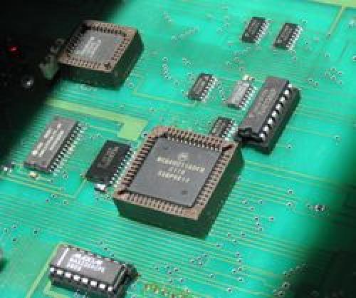
| − | ** | + | **The 6811 Processor: references |
| + | *** The official Motorola [http://maven.smith.edu/~thiebaut/classes/270/6811/68hc11a8.pdf 68HC11A8 Data Sheet]. Fairly cryptic... | ||
| + | *** A Motorola [[Media:6811Manual.pdf | 6811 Manual]]. It is a nicely written refresher on many concepts of assembly language applied to the 6811. | ||
| + | **** Check Section 3.2 on addressing modes (inherent, direct, extended, indexed, relative). | ||
| + | **** Get a refresher for the different instruction types (arithmetic, shifts, control, etc) in Section 3.4. | ||
| + | **** The condition code register is covered in Section 3.5. Skip Section 4. | ||
| + | *** [http://maven.smith.edu/~thiebaut/classes/270/6811/68hc11ref-2002.pdf M68HC11 Technical Reference], from Motorola. | ||
| + | ****Section 6.5 shows the instructions in logical groups. | ||
| + | ** [http://maven.smith.edu/~thiebaut/classes/270/6811/68hc11pocket.pdf M68HC11 Pocket Reference]. | ||
| + | ***Very useful, on Page 15, a list of all the opcodes supported by the 6811, in numerical (hex) order. | ||
| + | ** [http://maven.smith.edu/~thiebaut/classes/270/6811/68hc11a8ref.pdf 68HC11A8 Technical Reference]: a hardware & engineering description. of the 6811, its ports, and how it operates. | ||
| + | **** See Section 10 for a cycle-by-cycle description of the execution of each instruction. | ||
| + | **** See Appendix A, Figure A-14 for the timing diagram of a typical (multiplexed expansion) memory access. | ||
| + | ** [http://www.ele.uri.edu/Courses/ele205/6811-Instructions/index.html 6811 Instruction Set], with hexadecimal opcodes. A reverse map, from hex to instructions can be found [http://home.earthlink.net/~tdickens/68hc11/68hc11_opcode_map.html here.] | ||
| + | ** [[Media:CSC270_Assembly_Instructions.pdf | 2-Page List]] of all the 6811 Instructions | ||
| + | ** [http://www.aspisys.com/asm11.htm Software] for the 6811 | ||
| + | ** <font color="magenta">[http://maven.smith.edu/~thiebaut/classes/270/ETW3800_W6811CPU.pdf Heathkit ETW3800 Trainer manual (pdf)]</font> | ||
| + | ---- | ||
| + | ** Concentration on Assembly Language | ||
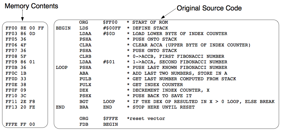
| + | ** [[CSC270 Example 6811 Program | Example]] of fully assembled 6800 program | ||
| + | ** [[Image:CSC270_6811_Listing_Format.png | 200 px | right ]] Listing format | ||
| + | *** opcodes, mnemonics, directives, columnar format | ||
| + | ** The instructions | ||
| + | ** Addressing Modes: inherent, immediate, direct, extended, indexed, relative | ||
* '''Wednesday''' | * '''Wednesday''' | ||
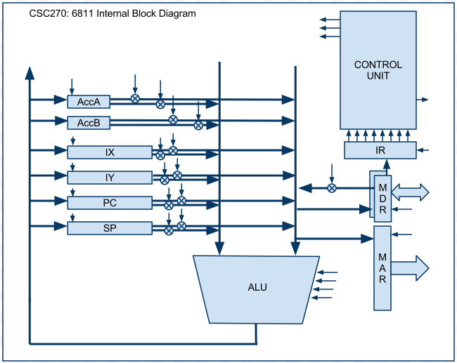
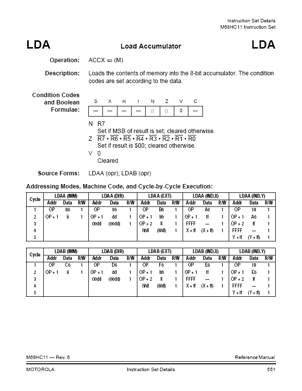
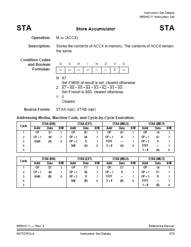
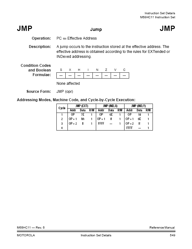
| + | ** A look at the internal circuits of the 6811. | ||
| + | [[Image:6811InternalALUCLU.png |200px]] | ||
| + | <br /> | ||
| + | [[Image:CSC270_LDAA.png|100px]] | ||
| + | [[Image:CSC270_STAA.png|100px]] | ||
| + | [[Image:CSC270_JMP.png|100px]] | ||
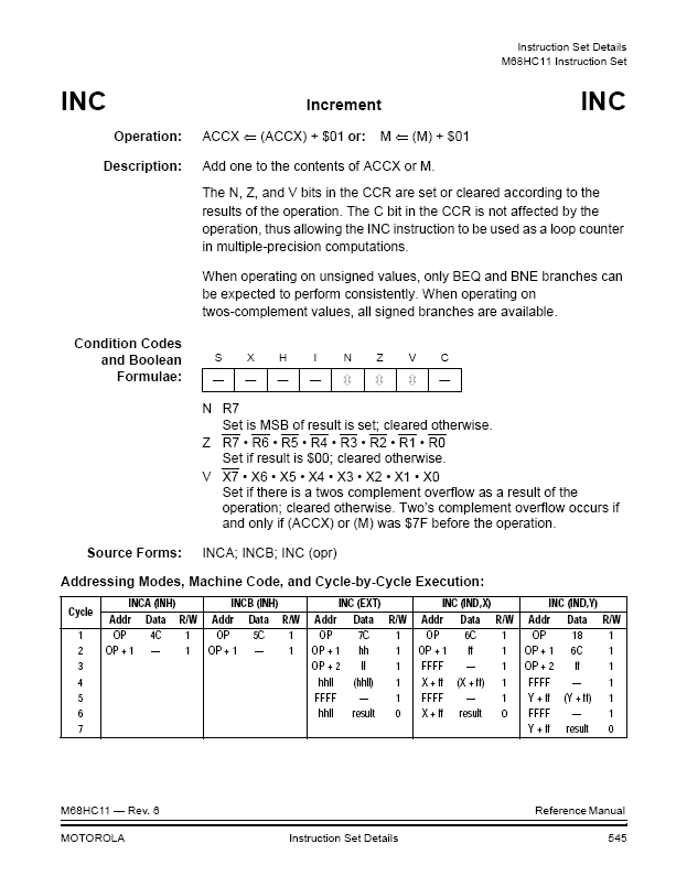
| + | [[Image:CSC270_INC.png|100px]] | ||
| + | <br /> | ||
* '''Friday''' | * '''Friday''' | ||
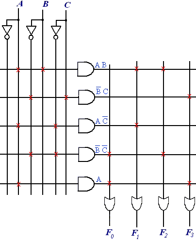
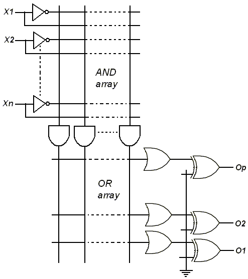
| + | ** Intro to Verilog | ||
| + | *** Images taken from http://www.cset.sp.utoledo.edu/eet3350/lesson1.html | ||
| + | [[Image:ProgrammableLogicArray1.gif|200px]][[Image:ProgrammableLogicAray2.gif|200px]] | ||
| + | <br /> | ||
| + | <videoflash>W1NZ01EEXvc</videoflash> | ||
| + | <br /> | ||
| + | ** Instruction Groups: data movement, arithmetic, logic, control, misc. | ||
| + | ** [[CSC270 6811 Programming Exercises | Programming Exercises]] | ||
| + | |||
---- | ---- | ||
| − | * | + | * [[CSC270_Lab_8_2011 | Lab #8 ]] |
| − | || | + | * [[CSC270_Homework_6 2011 | Homework #6]] |
| − | * | + | || |
| + | *Read the [[Media:6811Manual.pdf |6811 Manual ]] for this week. Quiz on Monday 3/28/09 on this material. | ||
| + | *[http://maven.smith.edu/~thiebaut/classes/231_0708/crashcourse/ Crash course] on Assembly Language | ||
<!-- ================================================================== --> | <!-- ================================================================== --> | ||
| Line 177: | Line 329: | ||
* '''Monday''' | * '''Monday''' | ||
** lecture | ** lecture | ||
| − | ** lab | + | ** [[CSC270 Quiz on 6800| Quiz]] |
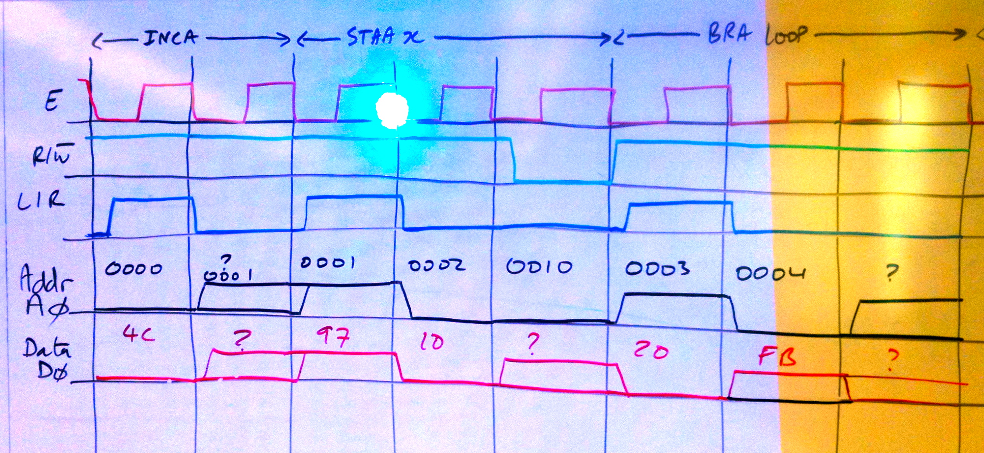
| − | * '''Wednesday''' | + | ** Cycle-by-cycle description of an endless loop of 3 instructions: |
| + | |||
| + | 0000 4C LOOP: INCA | ||
| + | 0001 97 10 STAA x | ||
| + | 0003 20 FB BRA LOOP | ||
| + | |||
| + | <center>[[Image:6811TimingDiagramOfLoop.jpg|300px]]</center> | ||
| + | ** [[CSC270 Lab 9 2011 | lab 9]] | ||
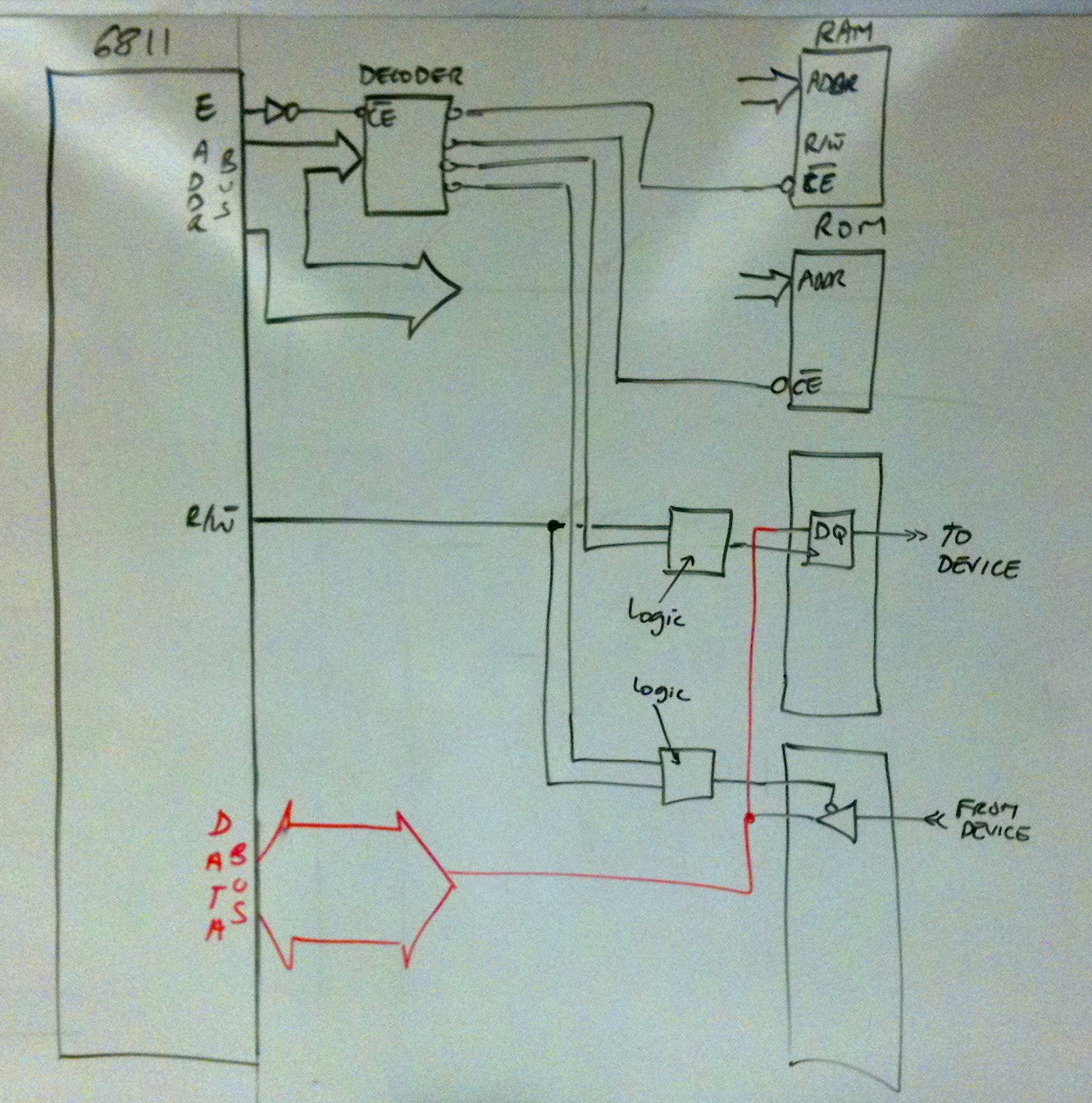
| + | * '''Wednesday''': '''MEMORY-MAPPED I/O''' | ||
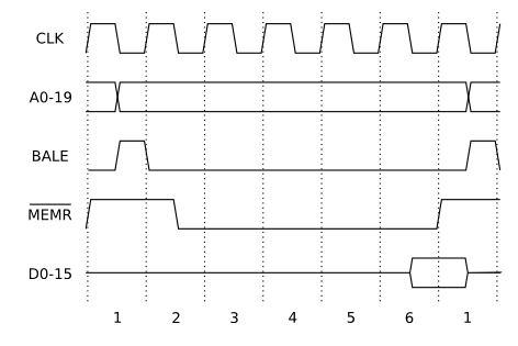
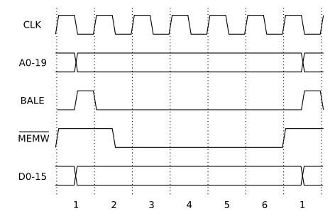
| + | ** Memory read/write cycles (taken from http://d3s.mff.cuni.cz/~ceres/sch/osy/text/ch01s03s02.html) | ||
| + | *** Memory Read<center>[[Image:CSC270ISAReadCycle.png|300px]]</center> | ||
| + | *** Memory Write<center>[[Image:CSC270ISAWriteCycle.png|300px]]</center> | ||
| + | ** Memory game: sticky notes + address bus + decoding | ||
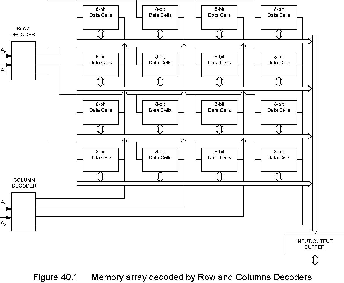
| + | ** Memory Bit-Array with decoders (Image taken from http://free-books-online.org/computers/digital-logic-design/decoding-large-memories/)<br /><center>[[Image:MemoryBitArrayWithDecoding.jpg|400px]] </center> | ||
| + | ** The idea behind ''Memory-Mapped I/O'' | ||
| + | <br /> | ||
| + | <!--center>[[Image:CSC270_6811MemoryMapExample.jpg| right| 150px]]</center--> | ||
| + | <br /> | ||
| + | <br /> | ||
| + | <br /> | ||
| + | <br /> | ||
| + | |||
* '''Friday''' | * '''Friday''' | ||
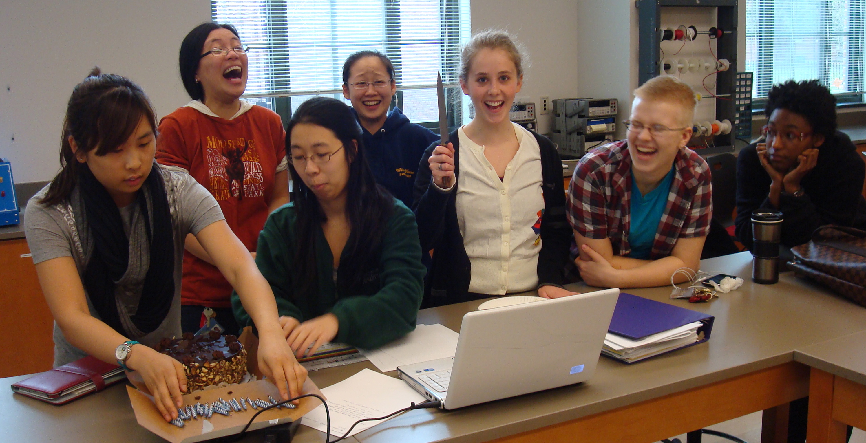
| + | ** Happy Birthday Edo! (all the pics on [http://www.facebook.com/album.php?fbid=10150149647311884&id=264041891883&aid=292188 Facebook]) | ||
| + | <center>[[Image:BirthdayEdo040111.jpg|400px]]</center> | ||
---- | ---- | ||
| − | * | + | * [[CSC270 Lab 9 2011 | lab 9]] |
|| | || | ||
* | * | ||
| Line 188: | Line 363: | ||
| Week 11 <br /> 4/4 | | Week 11 <br /> 4/4 | ||
|| | || | ||
| + | [[Image:6811KitMemoryMap.png|100px|right]] | ||
| + | [[Image:6811_addressDecoding.png|150px|right]] | ||
| + | <!--[[Image:ParisMinistryFaradayCage.jpg|100px|right]]--> | ||
* '''Monday''' | * '''Monday''' | ||
| − | ** lecture | + | ** lecture: |
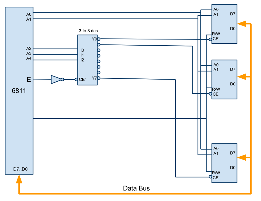
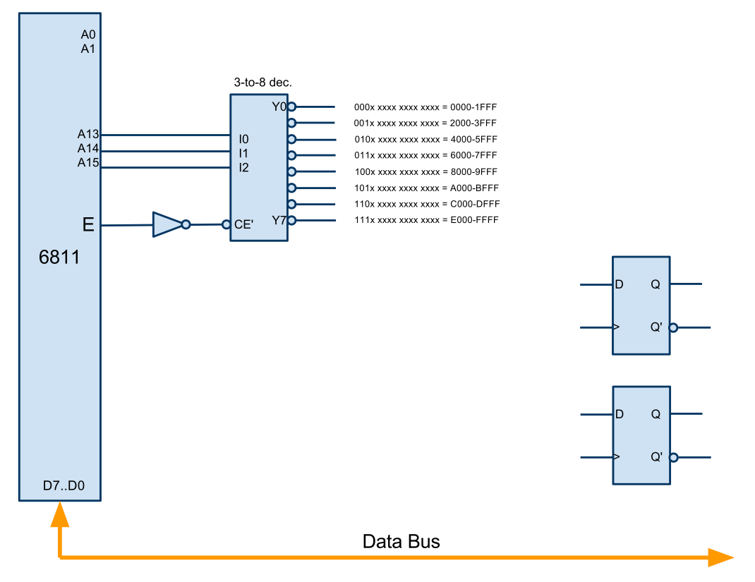
| + | *** address decoding | ||
| + | *** full vs. partial address decoding | ||
| + | *** the concept of a '''memory-mapped I/O''' system | ||
| + | *** [[CSC270 Exercises on Memory-Mapped I/O | Exercises]] | ||
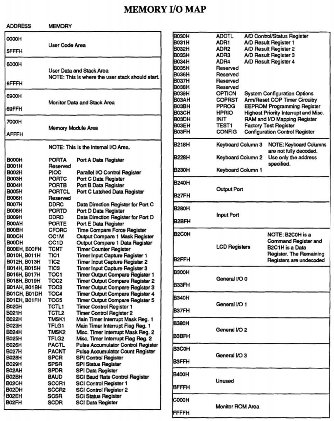
| + | *** Memory map of the 6811 kit (Page 49 of the <font color="magenta">[http://maven.smith.edu/~thiebaut/classes/270/ETW3800_W6811CPU.pdf Heathkit ETW3800 Trainer manual (pdf)]</font> | ||
** lab | ** lab | ||
| − | * '''Wednesday''' | + | *** [[CSC270 Lab 10 2011 | Lab 10]] |
| + | * '''Wednesday'''[[Image:CSC270_2_Bit_IO.png|right|150px]] | ||
| + | ** [[CSC270 Memory-Mapped I/O Exercises| Designing a 2-bit I/O port]]: 2 solutions | ||
| + | *** Parallel-write design (the 2 bits have the same address) | ||
| + | *** Separate-address design (the 2 bits have different addresses) | ||
| + | ** Continue with [[CSC270 Lab 10 2011 | Lab 10]] | ||
* '''Friday''' | * '''Friday''' | ||
| + | <br /> | ||
| + | <br /> | ||
| + | <br /> | ||
| + | <br /> | ||
| + | <br /> | ||
| + | <br /> | ||
| + | |||
---- | ---- | ||
| − | * | + | * [[CSC270 Lab 10 2011 | Lab 10]] |
| + | * [[CSC270 Homework 7 2011 | Homework 7]] <font color="magenta"><-- due 4/16 midnight</font> | ||
|| | || | ||
| − | * | + | * [http://en.wikipedia.org/wiki/Memory-mapped_I/O Memory-Mapped I/O] in Wikipedia |
<!-- ================================================================== --> | <!-- ================================================================== --> | ||
|- style="background:#eeeeff" valign="top" | |- style="background:#eeeeff" valign="top" | ||
| Week 12 <br /> 4/11 | | Week 12 <br /> 4/11 | ||
|| | || | ||
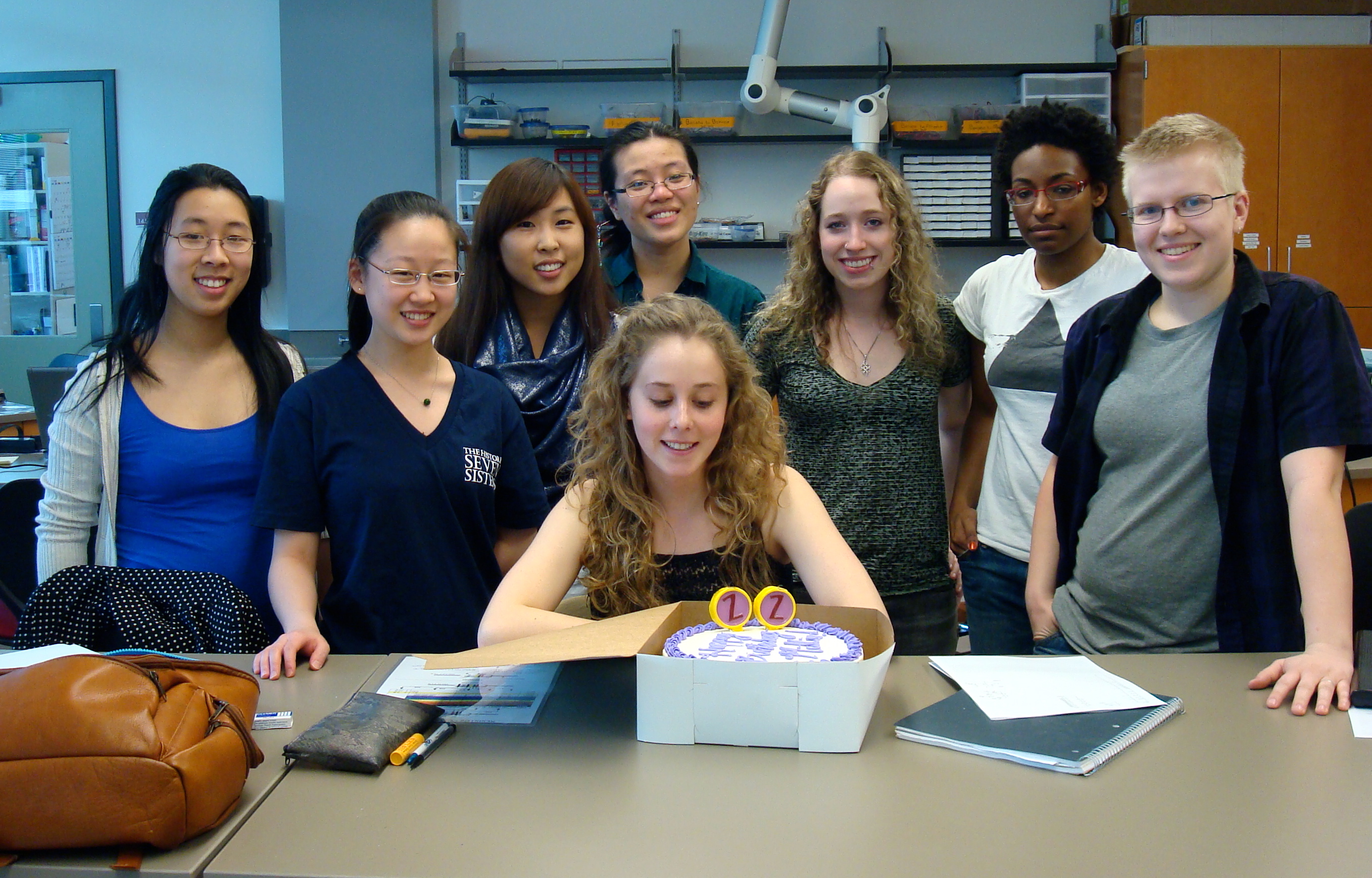
| + | * Happy Birthday Millie! (all pictures on [http://www.facebook.com/album.php?fbid=10150157690196884&id=264041891883&aid=294850 Facebook].) | ||
| + | <center> | ||
| + | [[Image:HappyBirthdayMillie.jpg|400px]] | ||
| + | </center> | ||
| + | <br /> | ||
| + | [[Image:74240.png|100px|right ]] | ||
| + | [[Image:74244.png|100px|right ]] | ||
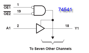
| + | [[Image:74541.png|100px|right ]] | ||
* '''Monday''' | * '''Monday''' | ||
** lecture | ** lecture | ||
| − | ** | + | *** the Input side of I/O with the 6811 |
| + | *** [[CSC270 Tri-State Drivers|Tri-State Drivers]] (a review) | ||
| + | ** [[CSC270 Lab 11 2011 | Lab 11 ]] | ||
| + | *** Designing and wiring up an input port with the 6811 | ||
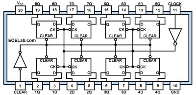
| + | [[Image:74273Register.jpg|150px|right]] | ||
| + | [[Image:74166ShiftRegister.gif|150px|right]] | ||
* '''Wednesday''' | * '''Wednesday''' | ||
| − | * '''Friday''' | + | [[Image:CSC270_6811IOScheme.jpg|100px|right]] |
| + | ** How to figure out how many different addresses energize Y4? | ||
| + | ** Examples of I/O Ports | ||
| + | *** Parallel Port | ||
| + | **** Data Registers | ||
| + | **** Control Registers | ||
| + | **** Status Registers | ||
| + | **** Handshake Protocol | ||
| + | **** Software Driver | ||
| + | |||
| + | * '''Friday''': '''<font color="magenta">No class: Programming Contest!</font>''' | ||
---- | ---- | ||
| − | * | + | * [[CSC270 Lab 11 2011 | Lab 11 ]] |
|| | || | ||
| − | * | + | * [[Media:6811_MemoryMappedIO.pdf | Input/Output with the 6811: Memory-Mapped I/O]] |
<!-- ================================================================== --> | <!-- ================================================================== --> | ||
|- style="background:#ffffff" valign="top" | |- style="background:#ffffff" valign="top" | ||
| Week 13 <br /> 4/18 | | Week 13 <br /> 4/18 | ||
|| | || | ||
| − | * '''Monday''' | + | * '''Monday''' (in FH345: lab shared with Susan Voss's class) |
| − | ** | + | ** Lecture |
| − | ** lab | + | *** [[CSC270 Homework 8 2011 | Homework 8]] <--- <font color="magenta">due 4/25/11</font> |
| + | *** Serial Port ( [[media:74166DataSheet.pdf|74166 datasheet]]) | ||
| + | *** ROM-based sequencers | ||
| + | *** Attaching a RAM circuit to the 6811 ([[CSC270 Lab12 Board Photos 2011| photos]]) | ||
| + | ** [[CSC270 lab 12 2011 | Lab #12]] | ||
* '''Wednesday''' | * '''Wednesday''' | ||
| + | ** Continuation of [[CSC270 lab 12 2011 | Lab #12]] | ||
* '''Friday''' | * '''Friday''' | ||
| + | ** [[CSC270 Introduction to the Arduino | Introduction to the Arduino]] | ||
---- | ---- | ||
| − | * | + | * [[CSC270 Homework 8 2011 | Homework 8]] <--- <font color="magenta">due 4/25/11</font> |
| + | * [[CSC270 lab 12 2011 | Lab #12]] | ||
|| | || | ||
* | * | ||
| Line 227: | Line 453: | ||
| Week 14 <br /> 4/25 | | Week 14 <br /> 4/25 | ||
|| | || | ||
| + | * Please watch on your own the very good Arduino video. | ||
| + | <videoflashright type="vimeo">18539129</videoflashright> | ||
| + | <br /> | ||
| + | <br /> | ||
* '''Monday''' | * '''Monday''' | ||
| − | ** | + | ** [[CSC270_Introduction_to_the_Arduino | Lab #13]], the Arduino Lab: <font color="magenta">no report to write</font>. |
| − | + | * '''Wednesday''' <font color="magenta">'''[[CSC270 Final Exam 2011 |TAKE HOME FINAL]]'''</font> | |
| − | * '''Wednesday''' | + | * '''Friday''': TBA |
| − | |||
---- | ---- | ||
| − | * | + | * [[CSC270_Introduction_to_the_Arduino | Lab #13]] |
|| | || | ||
* | * | ||
|} | |} | ||
| − | + | ||
---- | ---- | ||
[[CSC270 2009 | Back]] To Main Page | [[CSC270 2009 | Back]] To Main Page | ||
| Line 243: | Line 472: | ||
=Links and Resources= | =Links and Resources= | ||
| + | |||
| + | =Research= | ||
| + | * Weird: [http://www.engadget.com/2011/10/24/scientists-build-logic-gates-out-of-gut-bacteria-then-hopefully/ scientists build elementary gates] with E-Coli... | ||
| + | |||
| + | ==Lab Reports for Labs 1 to 12== | ||
| + | <onlydft> | ||
| + | * Tiffany's reports for the year: [[Media:CSC270_LabReport1_2011.pdf | Lab 1]], [[Media:CSC270_LabReport2_2011.pdf | Lab 2]], [[Media:CSC270_LabReport3_2011.pdf | Lab 3]], [[Media:CSC270_LabReport4_2011.pdf | Lab 4]], [[Media:CSC270_LabReport5_2011.pdf | Lab 5]], [[Media:CSC270_LabReport6_2011.pdf | Lab 6]], [[Media:CSC270_LabReport7_2011.pdf | Lab 7]], [[Media:CSC270_LabReport8_2011.pdf | Lab 8]], [[Media:CSC270_LabReport9_2011.pdf | Lab 9]], [[Media:CSC270_LabReport10_2011.pdf | Lab 10]], [[Media:CSC270_LabReport11_2011.pdf | Lab 11]], and [[Media:CSC270_LabReport12_2011.pdf | Lab 12]]. | ||
| + | </onlydft> | ||
| + | |||
| + | ==Printing== | ||
| + | |||
| + | * How to print a text file (pure ASCII, not an MS Word document) from a beowulf account to the printer @ FH354: | ||
| + | |||
| + | cprint -15 myFile.txt | ||
| + | |||
| + | * How to print a pdf from a beowulf account to the printer @ FH354: | ||
| + | |||
| + | lpr -P ford354 max232.pdf | ||
| + | |||
| + | * How to print an image to the same printer, from a beowulf account: | ||
| + | |||
| + | convert myImage.jpg myImage.pdf | ||
| + | lpr -P ford354 myImage.pdf | ||
==Programs== | ==Programs== | ||
| − | * [[CSC270 GenerateTruthTable.py | | + | * [[CSC270 GenerateTruthTable.py | Python and Java programs]] that generates truth tables. |
==Software== | ==Software== | ||
| + | |||
| + | ===Free Circuit CAD Systems=== | ||
| + | * [http://sourceforge.net/apps/mediawiki/tinycad/index.php?title=TinyCAD TinyCAD] | ||
| + | <videoflashright>1B9sQGtt-5w</videoflashright> | ||
| + | <br /> | ||
| + | <br /> | ||
| + | <br /> | ||
| + | <br /> | ||
| + | <br /> | ||
| + | <br /> | ||
| + | <br /> | ||
| + | <br /> | ||
| + | <br /> | ||
| + | <br /> | ||
| + | <br /> | ||
| + | <br /> | ||
| + | <br /> | ||
| + | <br /> | ||
| + | <br /> | ||
| + | <br /> | ||
| + | <br /> | ||
| + | <br /> | ||
| + | <br /> | ||
| + | <br /> | ||
| + | <br /> | ||
| + | <br /> | ||
| + | |||
| + | |||
| + | * http://www.xmarks.com/site/www.tech-systems-labs.com/freesoftware.htm | ||
| + | |||
| + | ===PSpice 9=== | ||
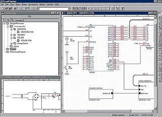
[[Image:pspice9.jpg | right | 200 px]] | [[Image:pspice9.jpg | right | 200 px]] | ||
| − | |||
* Pspice 9, Student version. An nice alternative to drawing schematics by hand. | * Pspice 9, Student version. An nice alternative to drawing schematics by hand. | ||
* This is a '''Windows''' version. (I have tried to make it work under wine/Mac OS X but haven't been able to make it load the libraries correctly) | * This is a '''Windows''' version. (I have tried to make it work under wine/Mac OS X but haven't been able to make it load the libraries correctly) | ||
| Line 286: | Line 568: | ||
** See Section 10 for a cycle-by-cycle description of the execution of each instruction. | ** See Section 10 for a cycle-by-cycle description of the execution of each instruction. | ||
** See Appendix A, Figure A-14 for the timing diagram of a typical (multiplexed expansion) memory access. | ** See Appendix A, Figure A-14 for the timing diagram of a typical (multiplexed expansion) memory access. | ||
| − | + | * <font color="magenta">[http://maven.smith.edu/~thiebaut/classes/270/ETW3800_W6811CPU.pdf Heathkit ETW3800 Trainer manual (pdf)]</font> | |
| + | * [[Media:6811_MemoryMappedIO.pdf | Input/Output with the 6811: Memory-Mapped I/O]] (Heathkit documentation) | ||
<br /> | <br /> | ||
<br /> | <br /> | ||
Latest revision as of 11:50, 15 January 2016
--D. Thiebaut 08:44, 7 January 2011 (EST)
Back to Main Page for CSC270
Contents
Prof
|
Dominique Thiébaut email |
Weekly Schedule
First 1/2 of Semester
| Week | Topics | Reading |
| Week 1 1/24 |
|
|
| Week 2 1/31 |
|
|
| Week 3 2/7 |
|
|
| Week 4 2/14 |
|
|
| Week 5 2/21 |
|
|
| Week 6 2/28 |
|
|
| Week 7 3/7 |
|
|
| Week 8 3/14 |
 |
|
Second 1/2 of Semester
| Week | Topics | Reading |
| Week 9 3/21 |
|
|
| Week 10 3/28 |
    0000 4C            LOOP:  INCA
    0001 97 10                STAA    x
    0003 20 FB                BRA      LOOP
 |
|
| Week 11 4/4 |
|
|
| Week 12 4/11 |
|
|
| Week 13 4/18 |
|
|
| Week 14 4/25 |
|
|
Back To Main Page
Links and Resources
Research
- Weird: scientists build elementary gates with E-Coli...
Lab Reports for Labs 1 to 12
Printing
- How to print a text file (pure ASCII, not an MS Word document) from a beowulf account to the printer @ FH354:
cprint -15 myFile.txt
- How to print a pdf from a beowulf account to the printer @ FH354:
lpr -P ford354 max232.pdf
- How to print an image to the same printer, from a beowulf account:
  convert myImage.jpg  myImage.pdf
  lpr -P ford354 myImage.pdf
Programs
- Python and Java programs that generates truth tables.
Software
Free Circuit CAD Systems
PSpice 9
- Pspice 9, Student version. An nice alternative to drawing schematics by hand.
- This is a Windows version. (I have tried to make it work under wine/Mac OS X but haven't been able to make it load the libraries correctly)
- Make sure you select the schematics option when installing the software.
- Select Tools/Schematics when starting the editor
- The schematics editor is located in C:\Program Files\OrCAD_Demo\PSpice\PDesign.exe upon installation.
- Download here!
- PSpice Tutorial
Integrated Circuit Data-Sheets
- Java Applets demonstrating most logical gates
- Texas Instruments and Harris Semiconductors' Data Sheet Search Engine
- Fairchild Semiconductors' Data Sheet Search Engine
- 74LS00, 74LS01, 74LS02, 74LS03, 74LS04, 74LS05, 74LS08, 74LS09, 74LS10, 74LS12, 74LS13, 74LS15, 74LS20, 74LS21, 74LS22, 74LS26, 74LS27, 74LS28, 74LS30, 74LS32, 74LS33, 74LS37, 74LS38, 74LS40, 74LS42, 74LS47, 74LS48, 74LS51, 74LS54, 74LS55, 74LS74, 74LS75, 74LS76, 74LS83, 74LS85, 74LS86, 74LS90, 74LS95, 74LS138, 74HCT240, 74LS243, 74HCT244, 74LS259, 74HCT541
- 9368
- 2114 1Kx4 RAM ( with timing information )
- Octal D-Flipflop (we do not have these chips in our current collection of chips)
Motorola 68HC11 Documentation
- Good source of info on the 6811.
- 6811 FAQs.
- The official Motorola | 68HC11A8 Data Sheet. Fairly cryptic...
- A Motorola 6811 Manual. It is a nicely written refresher on many concepts of assembly language applied to the 6811.
- Check Section 3.2 on addressing modes (inherent, direct, extended, indexed, relative).
- Get a refresher for the different instruction types (arithmetic, shifts, control, etc) in Section 3.4.
- The condition code register is covered in Section 3.5.
- M68HC11 Technical Reference, Motorola
- Section 6.5 shows the instructions in logical groups.
- M68HC11 Pocket Reference.
- Very useful, on Page 15, a list of all the opcodes supported by the 6811, in numerical (hex) order.
- 68HC11A8 Technical Reference: a hardware and engineering description. of the 6811, its ports, and how it operates.
- See Section 10 for a cycle-by-cycle description of the execution of each instruction.
- See Appendix A, Figure A-14 for the timing diagram of a typical (multiplexed expansion) memory access.
- Heathkit ETW3800 Trainer manual (pdf)
- Input/Output with the 6811: Memory-Mapped I/O (Heathkit documentation)
Back To Main Page
