Difference between revisions of "CSC270 Weekly Schedule 2012"
(→Demos of Various Circuit) |
(→Xilinx and CPLDs) |
||
| (106 intermediate revisions by the same user not shown) | |||
| Line 182: | Line 182: | ||
---- | ---- | ||
* [[CSC270 Lab 5 2012 | Lab #5]] | * [[CSC270 Lab 5 2012 | Lab #5]] | ||
| − | * [[CSC270 Homework 5 2012 | Homework #5]] | + | * [[CSC270 Homework 5 2012 | Homework #5]] and [[CSC270 Homework 5 Solution 2012 | Solution]] |
|| | || | ||
* Chapter 5: synchronous sequential logic | * Chapter 5: synchronous sequential logic | ||
| Line 192: | Line 192: | ||
|width="60%"| | |width="60%"| | ||
* '''Monday''' | * '''Monday''' | ||
| + | ** The JK Flip-Flop | ||
| + | ** [http://www.odyseus.nildram.co.uk/RFIC_Circuits_Files/JK-type.pdf diagram] | ||
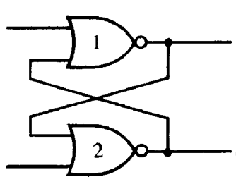
| + | ** '''Exercise 1''': Let's figure out how to design a FSM without external input first. | ||
| + | ** '''Exercise 2''': Same idea, with a user input. | ||
* '''Wednesday''' | * '''Wednesday''' | ||
| + | ** [[CSC270 JK Flip-flop Exercises | Exercises with the JK Flip-Flop]] | ||
| + | |||
* '''Friday''' | * '''Friday''' | ||
| + | ** [[CSC270 Midterm Prep 2012 | Midterm Prep]] | ||
---- | ---- | ||
| − | * | + | * [[CSC270 Lab 6 2012 | Lab #6]] |
| + | * [[CSC270 Homework 6 2012 | Homework #6]] | ||
|| | || | ||
| Line 204: | Line 212: | ||
|| | || | ||
* '''Monday''' | * '''Monday''' | ||
| − | * '''Wednesday''' : <font color="magent">Midterm Exam</font> | + | ** ROM-Based Sequencers ([http://www.allaboutcircuits.com/vol_4/chpt_16/3.html Good reference]) |
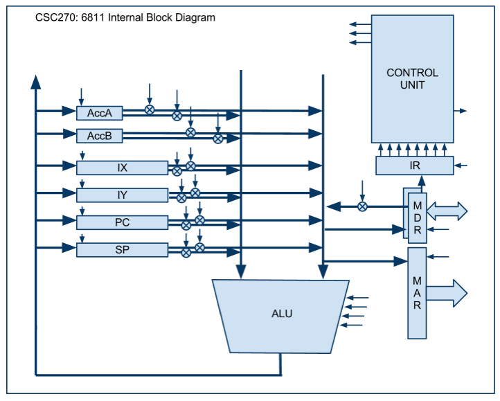
| + | ** [[Image:6811BlockDiagram.png|right|150px]] Introduction to the 6811. | ||
| + | * '''Wednesday''' : | ||
| + | ** <font color="magent">[[CSC270 Midterm Exam 2012 | Midterm Exam]]</font> | ||
| + | ** [[CSC270 Introduction to the 6811| Introduction to the 6811]] | ||
* '''Friday''' | * '''Friday''' | ||
| + | ** R&R | ||
| + | <br /> | ||
| + | <br /> | ||
| + | <br /> | ||
| + | <br /> | ||
| + | <br /> | ||
| + | <br /> | ||
| + | <br /> | ||
| + | <br /> | ||
---- | ---- | ||
| − | * | + | * |
|| | || | ||
* | * | ||
| + | |} | ||
| + | |||
<!-- ================================================================== --> | <!-- ================================================================== --> | ||
| − | |- valign="top" | + | <!--|- valign="top" |
| Week 9 <br /> 3/19<br /> | | Week 9 <br /> 3/19<br /> | ||
|| | || | ||
| Line 223: | Line 246: | ||
|} | |} | ||
| − | + | --> | |
| + | <br /> | ||
| + | [[Image:SpringBreak.png|800px]] | ||
| + | <br /> | ||
==Second Half == | ==Second Half == | ||
| Line 232: | Line 258: | ||
<!-- ================================================================== --> | <!-- ================================================================== --> | ||
|-valign="top" | |-valign="top" | ||
| − | | Week | + | |width="15%"| Week 1 <br /> 3/26 <br />[[Image:whiteSpace3.png]] |
| − | | | + | |width="60%"| |
* '''Monday''' | * '''Monday''' | ||
| + | ** [[CSC270 Introduction to the 6811| Review of 6811]] | ||
| + | ** Mini Lab (at end of [[CSC270 Introduction to the 6811| Intro to 6811]]) | ||
| + | ** Comments on past [[CSC270 Midterm Exam 2012|Midterm ]] | ||
* '''Wednesday''' | * '''Wednesday''' | ||
| + | ** [[CSC270 Exercises on Assembly Language | Learning Assembly through Exercises]] | ||
* '''Friday''' | * '''Friday''' | ||
| + | ** Office Hours | ||
| + | <br /> | ||
| + | <br /> | ||
---- | ---- | ||
| − | * | + | * [[CSC270 Lab 7 2012 | Lab 7]] (first part done on Monday. Second part on Wednesday) |
| + | * [[CSC270 Homework 7 2012 | Homework 7]] and [[CSC270 Homework 7 Solution 2012| Solution]] | ||
| + | |||
|| | || | ||
| − | * | + | * Reading: |
| + | ** [http://www.clear.rice.edu/elec201/Book/6811_asm.html A good tutorial on 6811 assembly language] ([[Media:6811AssemblyTutorial_RiceUniversity.pdf|pdf]]) | ||
| + | ** Feel free to also sample the information in the [[CSC270_Introduction_to_the_6811#References|References]] section of the [[CSC270_Introduction_to_the_6811 | Introduction to the 6800]] we saw in class. | ||
| + | <br /> | ||
| + | |||
| + | [[Image:whiteSpace2.png]] | ||
<!-- ================================================================== --> | <!-- ================================================================== --> | ||
|- style="background:#eeeeff" valign="top" | |- style="background:#eeeeff" valign="top" | ||
| Line 247: | Line 287: | ||
|| | || | ||
* '''Monday''' | * '''Monday''' | ||
| + | ** The process of disassembling: [[CSC270 Exercise on Disassembling| Disassembling Exercise]] | ||
| + | ** Indexed Addressing Mode | ||
| + | |||
| + | |||
| + | ** Conditional Branches. | ||
| + | *** BEQ, BNE, BGT (signed), BLT (signed) | ||
| + | *** A good dec/hex converter that works with signed numbers: [http://www.binaryconvert.com/convert_signed_char.html binaryconvert.com] | ||
* '''Wednesday''' | * '''Wednesday''' | ||
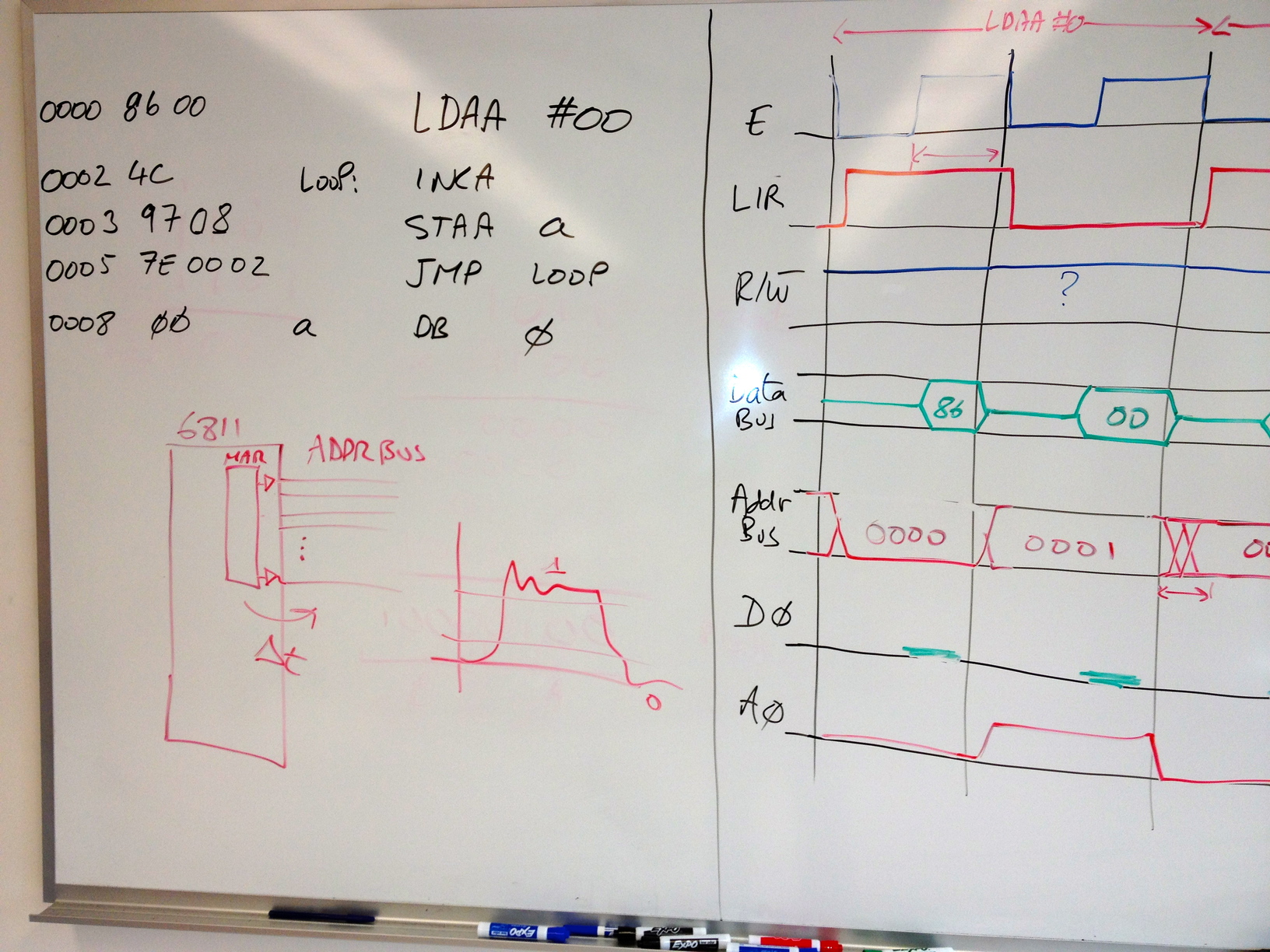
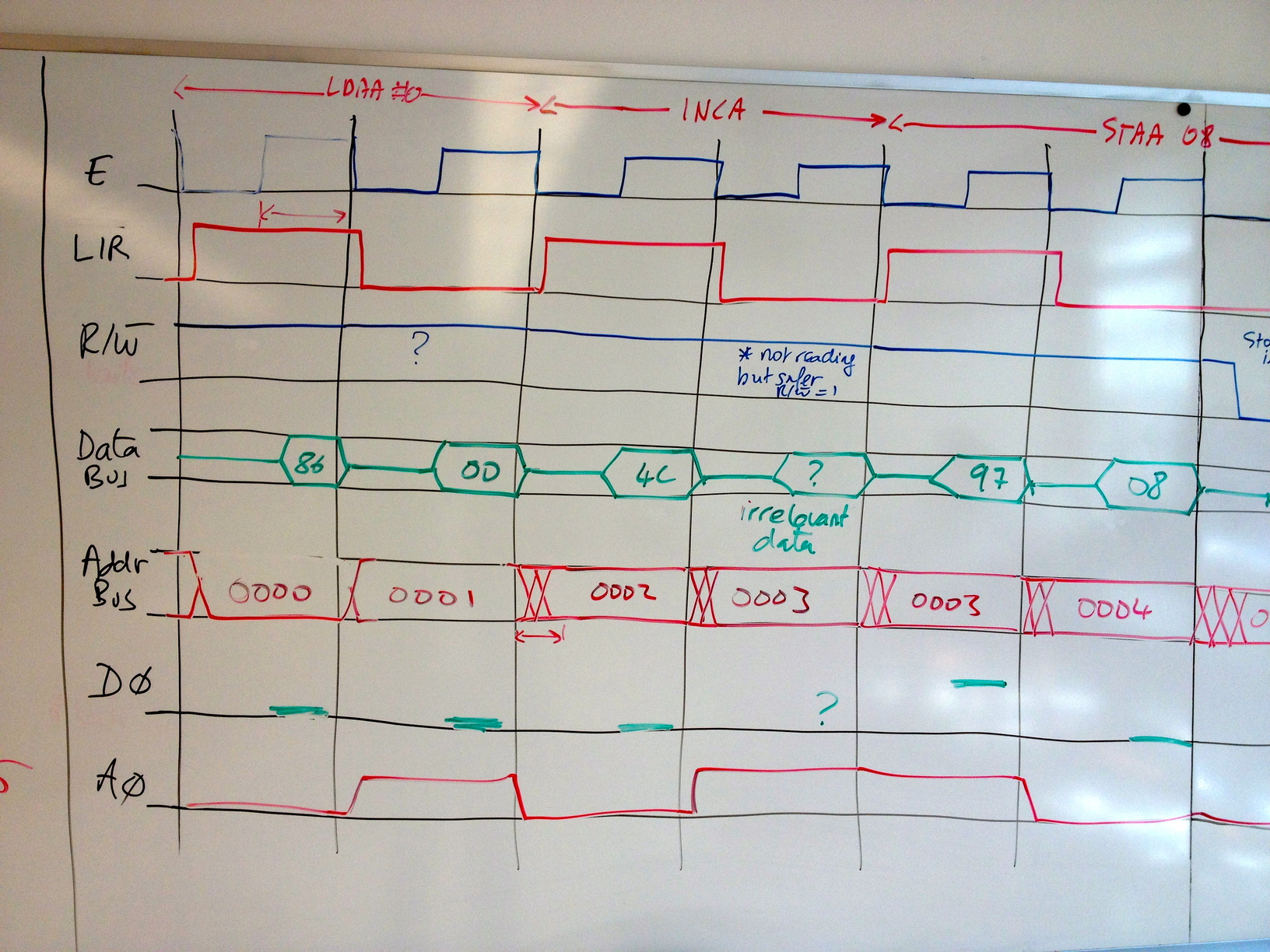
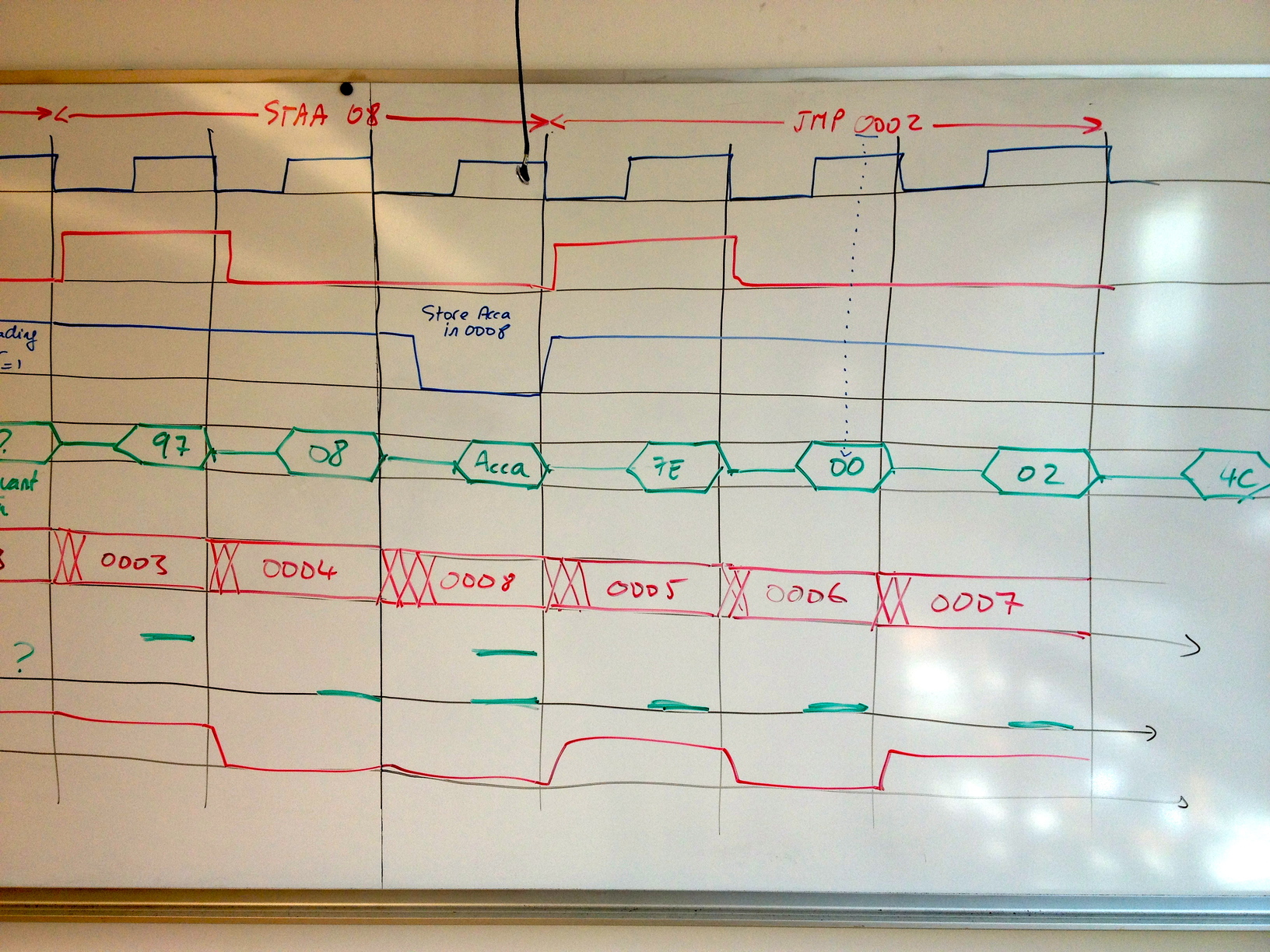
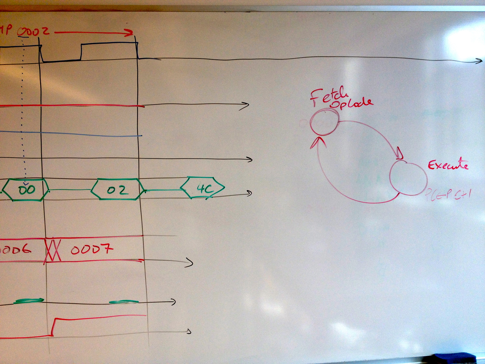
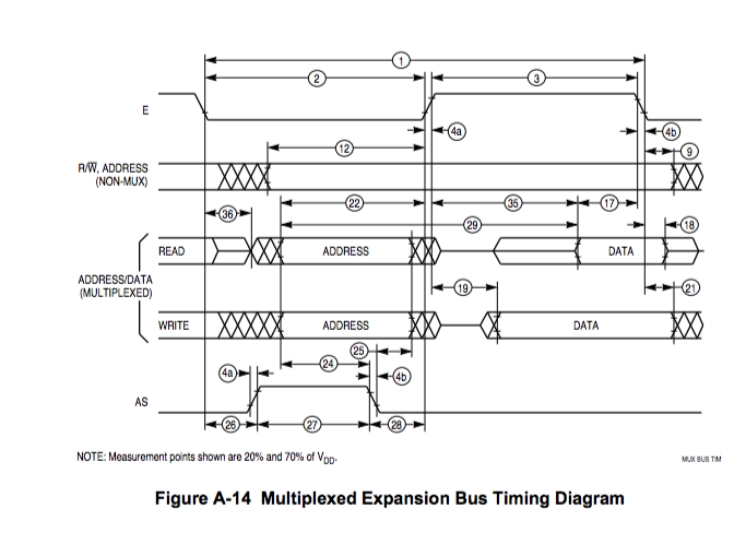
| + | ** Engineering: Deciphering how the 6811 energizes the Address, Data and Control busses when it runs a program. | ||
| + | <center>[[Image:CSC270_FigureA14.png|200px]] [[Image:CSC270_TableFigureA14.png|200px]] <br /> (taken from [http://maven.smith.edu/~thiebaut/classes/270/6811/68hc11a8ref.pdf the 6811 Reference Manual])</center> | ||
| + | ** The main signals: E, R/W, and LIR | ||
| + | <center>[[Image:6811MainSignalsE_RW_LIR.png|200px]]</center> | ||
| + | ** Screen shots: | ||
| + | {| | ||
| + | | | ||
| + | [[Image:CSC270TimingDiagramLoop1.jpg|100px]] | ||
| + | | | ||
| + | [[Image:CSC270TimingDiagramLoop2.jpg|100px]] | ||
| + | | | ||
| + | [[Image:CSC270TimingDiagramLoop3.jpg|100px]] | ||
| + | | | ||
| + | [[Image:CSC270TimingDiagramLoop4.jpg|100px]] | ||
| + | |} | ||
| + | |||
* '''Friday''' | * '''Friday''' | ||
| + | ** Sentence of the week, found in the 6811 Pocket Reference: <blockquote><font color="magenta">The term ''Big Endian'' comes from Jonathan Swift’s satire Gulliver’s Travels. In Swift’s book, a Big Endian refers to a person who cracks their egg on the big end. The Lilliputians considered the big endians as inferiors. The big endians fought a long and senseless war with the Lilliputians who insisted it was only proper to break an egg on the little end.</font></blockquote> | ||
| + | ** Negative numbers in binary | ||
| + | ** Condition Codes: HINZVC | ||
| + | *** Z: Zero | ||
| + | *** V: Overflow | ||
| + | *** N: Negative | ||
| + | *** C: Carry | ||
| + | *** H: Half-Carry | ||
| + | *** I: Interrrupt Mask | ||
| + | ** Conditional Branches | ||
| + | *** BEQ | ||
| + | *** BNE | ||
| + | *** BGT | ||
| + | *** BLT | ||
| + | *** BRA (unconditional) | ||
---- | ---- | ||
| − | * | + | * [[CSC270 Lab 8 2012| Lab 8]] |
| + | * [[CSC270 Homework 8 2012 | Homework 8]] | ||
|| | || | ||
| − | * | + | * Negative (signed) numbers are covered in the [http://cs.smith.edu/dftwiki/images/4/47/6811Manual.pdf 6811 Manual], In Section 3. |
| + | * The Condition Code register is also covered in Section 3. | ||
<!-- ================================================================== --> | <!-- ================================================================== --> | ||
|- style="background:#ffffff" valign="top" | |- style="background:#ffffff" valign="top" | ||
| Line 258: | Line 338: | ||
|| | || | ||
* '''Monday''' | * '''Monday''' | ||
| + | ** Review of negative numbers. | ||
| + | ** New question: How can we extend a positive or negative number from 1 byte to two bytes? | ||
| + | ** Review Condition Code Register | ||
| + | ** Rule: | ||
| + | *** Every instruction that makes information pass through ALU will modify the CC bits (HINZVC). Typical instructions: Add, Sub, Shift, Rotate, Multiply, Divide, And, Or, Not, Xor, and '''Compare''' (which is a subtract operation). | ||
| + | *** Special instructions can modify individual bits: For example '''CLC''' and '''SEC''' can be used to clear or set the '''Carry''' bit. | ||
| + | *** Some instruction can have different outcome depending on some of the CC bits: ''Conditional Branches'': BEQ, BNE, BLT, BGT. | ||
| + | ** The '''Compare''' (CMP) instruction: | ||
| + | *** It is a subtract operation that does not store the result of the subtraction, but instead sets the HINZVC bit depending on the result of the subtraction. | ||
| + | ** The Conditional Branch instructrions: | ||
| + | *** They operate as follows: | ||
| + | |||
| + | if ''specific CC bit'' == ''some predefined value'': | ||
| + | PC = PC + ''displacement'' | ||
| + | else: | ||
| + | PC = PC + 1 | ||
| + | |||
| + | :::For example: | ||
| + | |||
| + | BEQ, (Branch if equal) | ||
| + | if Z bit == 1: | ||
| + | PC = PC + ''displacement'' | ||
| + | else: | ||
| + | PC = PC + 1 | ||
| + | |||
| + | *** Computing the displacement in hex. Case #1 | ||
| + | |||
| + | LDAA alpha | ||
| + | CMPA #5 ; alpha==5? | ||
| + | BEQ same | ||
| + | diff: ... ; go here if != 5 | ||
| + | ... | ||
| + | ... | ||
| + | same: ... ; go here if == 5 | ||
| + | |||
| + | :::Assume BEQ is at Address 0010 and ''same'' at Address ''0023''. Address of ''diff'' label is at 0012 (because BEQ label takes 2 bytes). 0012 + displacement must be equal to 0023. Hence displacement is 11 (only 2 digits, as only 1-byte displacement allowed). | ||
| + | |||
| + | *** Case #2: branching back | ||
| + | |||
| + | same: ... ; go here if == 5 | ||
| + | |||
| + | LDAA alpha | ||
| + | CMPA #5 ; alpha==5? | ||
| + | BEQ same | ||
| + | diff: ... ; go here if != 5 | ||
| + | ... | ||
| + | ... | ||
| + | |||
| + | :::Assume BEQ is at address 0020, and ''same'' is at 0005. The displacement must be a negative number that, once added to 0022 (because that's the address of the instruction after BEQ), will result in 0005. | ||
| + | |||
| + | 0022 | ||
| + | + XXXX | ||
| + | --------- | ||
| + | 0005 | ||
| + | |||
| + | :::There are many different ways to compute XXXX. Which ever way we find, we find XXXX = FFE3, so the displacement is the lower byte, or '''E3'''. | ||
| + | |||
| + | |||
| + | |||
* '''Wednesday''' | * '''Wednesday''' | ||
| + | ** Class Quiz: | ||
| + | *** Question 1: We know how to build an 8-bit adder with gates. How do we build an 8-bit subtracter? | ||
| + | *** Question 2: How can we build an 8-bit module that either adds or subtracts depending on a single command signal? If the signal is 0, the module adds two 8-bit values. If the signal is 1, the module subtracts one from the other. | ||
| + | ** Building a 1-bit output '''port''' | ||
| + | ** The [[Media:6811MemoryMap.pdf| 6811-Kit Memory Map]] | ||
* '''Friday''' | * '''Friday''' | ||
| + | ** Question in need of answers: How many different addresses does your Lab-9 LED respond to? | ||
| + | ** Overview of [[CSC270 Homework 9 2012 | Homework #9]] | ||
| + | ** Continuation of [[CSC270 Lab 9 2012 | Lab #9]]. | ||
| + | |||
---- | ---- | ||
| − | * | + | * [[CSC270 Lab 9 2012 | Lab #9]] |
| + | * [[CSC270 Homework 9 2012 | Homework #9]] and [[CSC270 Homework 9 Solutions 2012| solutions]] | ||
|| | || | ||
| − | * | + | * Reading |
| + | ** The condition code register is covered in Section 3.5 of the Motorola [[Media:6811Manual.pdf | 6811 Manual]]. Skip Section 4. | ||
<!-- ================================================================== --> | <!-- ================================================================== --> | ||
| Line 270: | Line 420: | ||
|| | || | ||
* '''Monday''' | * '''Monday''' | ||
| + | ** Preparation for Friday's possible visit (parents/students in class) | ||
| + | ** A review of how memory-mapped I/O works (output). The general rules | ||
| + | ** Building an '''input''' port | ||
| + | *** Basic rules of electronics when circuits exchange information: | ||
| + | **** One source to many receivers (talk about [http://en.wikipedia.org/wiki/Fan-out fan-out]) | ||
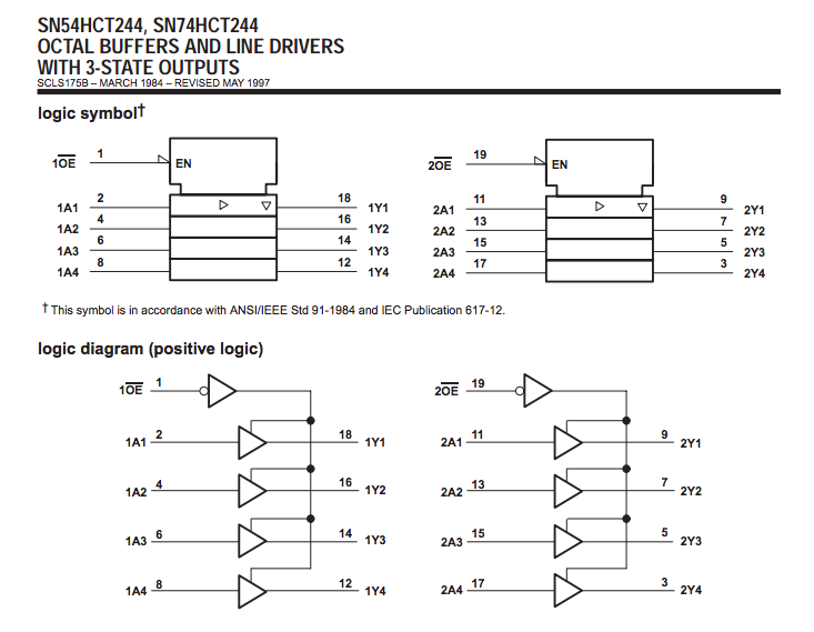
| + | **** Many sources to one receiver (talk about [http://en.wikipedia.org/wiki/Three-state_logic tristate drivers])<br /><center>[[Image:CSC270_244Driver.png|300px]]</center> | ||
| + | *** µP outputting data bit to many devices (ROM, RAM, I/O ports) | ||
| + | *** µP receiving data from several devices | ||
| + | *** Designing a 1-bit input port. The main players | ||
| + | *** The software driver for inputting the bit. | ||
| + | ** The alternative to '''memory-mapped I/O''': '''dedicated I/O''' | ||
* '''Wednesday''' | * '''Wednesday''' | ||
| + | [[Image:CentronicsProtocole.png|150px|right]] | ||
| + | ** Prepartion for [[CSC270 Lab 10 2012 | Lab #10]] | ||
| + | ** [[CSC270 Lab 10 2012 | Lab #10]] | ||
| + | ** Presentation of '''Dedicated I/O''' | ||
| + | ** Advantages and disadvantages of Dedicated vs. Memory-Mapped I/Os | ||
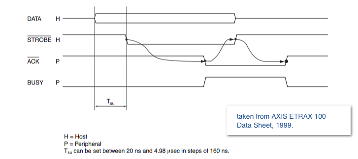
| + | ** The Centronics interface (explained in this [http://cs.smith.edu/dftwiki/images/1/1b/CSC270_ParallelPort.pdf pdf]). | ||
| + | ** [[CSC270 Exercises on 6811 I/O designs| Exercises]] | ||
* '''Friday''' | * '''Friday''' | ||
| + | ** If ( Class visit ) | ||
| + | *** Take a simple problem, develop it, wire it up, and demonstrate its good working conditions | ||
| + | ** else | ||
| + | *** { | ||
| + | **** Present current [[CSC270 Homework 10 2012 | homework assignment]] | ||
| + | **** <font color="magenta">'''Question of the day''': ''Why couldn't you set the LED from the keyboard in the one before the last lab?''</font> | ||
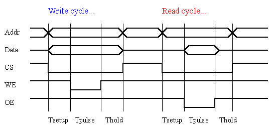
| + | **** Adding RAM to the 6811. The [http://maven.smith.edu/~thiebaut/classes/270/datasheets/nte2114.pdf 2114] 1Kx4 static RAM chip.<br />[[Image:2114TimingDiagram.gif|400px]]<br />(image taken from [http://www.doulos.com/knowhow/verilog_designers_guide/models/simple_ram_model/ www.doulos.com]) | ||
| + | **** Observation: Interfacing 2114 to 6811 is almost pin-to-pin wiring. This is because 2114 designed to be compatible with most processors. This in turns forces manufacturer to design new hardware to be compatible with older parts ==> we are stuck in a generic type of architecture (which is based on von Neumann architecture at a higher-level). | ||
| + | *** } | ||
| + | <br /> | ||
| + | <br /> | ||
---- | ---- | ||
| + | * [[CSC270 Lab 10 2012 | Lab #10]] | ||
| + | * [[CSC270 Homework 10 2012 | Homework #10]] and [[CSC270 Homework 10 Solution 2012| solutions]] | ||
| + | |||
|| | || | ||
| − | * | + | * The [http://cs.smith.edu/dftwiki/images/1/1b/CSC270_ParallelPort.pdf Parallel Port] protocol (centronics interface). |
| + | * [http://en.wikipedia.org/wiki/Memory-mapped_I/O Memory-Mapped I/O] on wikipedia | ||
| + | * [http://en.wikipedia.org/wiki/Memory-mapped_I/O Channel I/O]: when dedicated I/O goes the full length! | ||
<!-- ================================================================== --> | <!-- ================================================================== --> | ||
| Line 280: | Line 464: | ||
| Week 13 <br /> 4/23<br /> | | Week 13 <br /> 4/23<br /> | ||
|| | || | ||
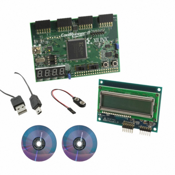
| + | [[File:CoolRunner-II kit.jpg|right|150px]] | ||
* '''Monday''' | * '''Monday''' | ||
| + | ** Review of the last homework assignment | ||
| + | ** Review of last lab: setting two LEDs to blink | ||
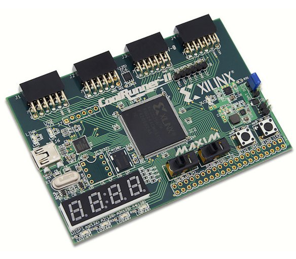
| + | ** Introduction to Xilinx's CPLD II, Xilinx's ISE 13.4, and the CoolRunner II kit. | ||
| + | ** <onlysmith>[http://cs.smith.edu/dftwiki/images/CPLDandVerilog.pdf Presentation (PDF)]</onlysmith> | ||
* '''Wednesday''' | * '''Wednesday''' | ||
| + | ** Xilinx ISE: <onlysmith>[http://cs.smith.edu/dftwiki/images/CPLDandVerilog.pdf Presentation #2 (PDF)]</onlysmith> | ||
* '''Friday''' | * '''Friday''' | ||
| + | ** [http://www.ccscne.org/2012/ CCSCNE Conference] | ||
---- | ---- | ||
| − | * | + | * [[CSC270 Lab 11 2012 | Lab #11 on Xilinx ISE and Schematics]] |
| + | * [[CSC270 Homework 11 2012 | Homework #11]] | ||
|| | || | ||
| − | * | + | * Good reference on Verilog: [http://ehis.ebscohost.com/eds/detail?vid=2&hid=20&sid=30d789de-3182-423d-9db9-da9edf403f24%40sessionmgr15&bdata=JnNpdGU9ZWRzLWxpdmU%3d#db=cat00321a&AN=fivecol.004029166 Fundamentals of DIgital Logic with Verilog Design], by Brown & Vranesic, McGraw Hill pub., 2003. |
<!-- ================================================================== --> | <!-- ================================================================== --> | ||
| Line 293: | Line 485: | ||
|| | || | ||
* '''Monday''' | * '''Monday''' | ||
| + | ** Introduction to Verilog. <onlysmith>[http://cs.smith.edu/dftwiki/images/IntroductionToVerilog.pdf Presentation Slides (PDF)]</onlysmith> | ||
* '''Wednesday''': <font color="magenta">Last Day of Class</font> | * '''Wednesday''': <font color="magenta">Last Day of Class</font> | ||
| + | ** Continuation of Verilog presentation. We stopped at Exercise 1 on Monday. We continue from there... | ||
| + | ** Presentation of the [[CSC270_Final_Exam_2012 | Final Exam]]. | ||
---- | ---- | ||
| + | * [[CSC270_Final_Exam_2012 | Take-Home Final Exam]] | ||
|| | || | ||
| − | * | + | * All the references for this week's material can be found at the bottom of this page, in the Xilinx and Verilog sections. |
| Line 327: | Line 523: | ||
==Programs== | ==Programs== | ||
| − | * [[CSC270 GenerateTruthTable.py | A Python program]] that generates a truth table. | + | * [[CSC270_Python_Operators_for_Simulation | How to implement AND, OR, NOT and simple logic circuits]] in Python |
| + | * [[CSC270 GenerateTruthTable.py | A Python program]] that generates a truth table. | ||
| + | * [[CSC270_GYRSequencer.py | A Python program]] to simulate a simple sequencer. | ||
==Software== | ==Software== | ||
===Demos of Various Circuit=== | ===Demos of Various Circuit=== | ||
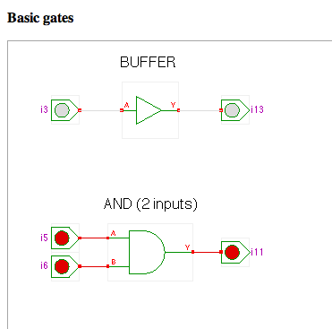
| − | [[Image:HadesGate. | + | [[Image:HadesGate.png| right ]] |
* [http://tams-www.informatik.uni-hamburg.de/applets/hades/webdemos/index.html Hades] at U. of Hamburg. | * [http://tams-www.informatik.uni-hamburg.de/applets/hades/webdemos/index.html Hades] at U. of Hamburg. | ||
<br /> | <br /> | ||
<br /> | <br /> | ||
| + | <br /> | ||
| + | <br /> | ||
| + | <br /> | ||
| + | <br /> | ||
| + | <br /> | ||
| + | <br /> | ||
| + | <br /> | ||
| + | <br /> | ||
| + | <br /> | ||
| + | <br /> | ||
| + | <br /> | ||
<br /> | <br /> | ||
| Line 355: | Line 564: | ||
===Free Circuit CAD Systems=== | ===Free Circuit CAD Systems=== | ||
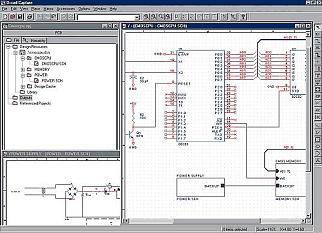
| + | * [https://www.circuitlab.com/ CircuitLab] | ||
| + | {| | ||
| + | |- valign="top" | ||
| + | | | ||
| + | (the video shows an analog circuit, but logic gates are also supported) | ||
| + | | | ||
| + | <videoflashright>f52GV1IpwVk</videoflashright> | ||
| + | |} | ||
| + | <br /> | ||
| + | <br /> | ||
| + | <br /> | ||
| + | |||
* [http://sourceforge.net/apps/mediawiki/tinycad/index.php?title=TinyCAD TinyCAD] | * [http://sourceforge.net/apps/mediawiki/tinycad/index.php?title=TinyCAD TinyCAD] | ||
<videoflashright>1B9sQGtt-5w</videoflashright> | <videoflashright>1B9sQGtt-5w</videoflashright> | ||
| Line 407: | Line 628: | ||
== Motorola 68HC11 Documentation== | == Motorola 68HC11 Documentation== | ||
[[Image:6811.jpg | right]] | [[Image:6811.jpg | right]] | ||
| − | * [http://www.eecs.ucf.edu/undergrad/CpE/labs/EEL4767 Good source of info] on the 6811. | + | <!-- *[http://www.eecs.ucf.edu/undergrad/CpE/labs/EEL4767 Good source of info] on the 6811. --> |
| + | * [http://www.ele.uri.edu/Courses/ele205/6811-Instructions/index.html A concise 2-page] list of the Instructions and op-codes. | ||
| + | * [http://www.clear.rice.edu/elec201/Book/6811_asm.html A good tutorial on 6811 assembly language] ([[Media:6811AssemblyTutorial_RiceUniversity.pdf|pdf]]) | ||
* [http://www.faqs.org/faqs/microcontroller-faq/68hc11/ 6811 FAQs]. | * [http://www.faqs.org/faqs/microcontroller-faq/68hc11/ 6811 FAQs]. | ||
| − | * The official Motorola [http://cs.smith.edu/~thiebaut/classes/270/6811/68hc11a8.pdf | + | * The official Motorola [http://cs.smith.edu/~thiebaut/classes/270/6811/68hc11a8.pdf 68HC11A8 Data Sheet]. Fairly cryptic... |
* A Motorola [http://www.handyboard.com/techdocs/6811intr.pdf 6811 Manual]. It is a nicely written refresher on many concepts of assembly language applied to the 6811. | * A Motorola [http://www.handyboard.com/techdocs/6811intr.pdf 6811 Manual]. It is a nicely written refresher on many concepts of assembly language applied to the 6811. | ||
** Check Section 3.2 on addressing modes (inherent, direct, extended, indexed, relative). | ** Check Section 3.2 on addressing modes (inherent, direct, extended, indexed, relative). | ||
| Line 425: | Line 648: | ||
<br /> | <br /> | ||
<br /> | <br /> | ||
| + | ==Verilog/CPLD== | ||
| + | [[File:CoolRunner-II_kit2.jpg|right|300px]] | ||
| + | === Books === | ||
| + | * Good reference on Verilog: [http://ehis.ebscohost.com/eds/detail?vid=2&hid=20&sid=30d789de-3182-423d-9db9-da9edf403f24%40sessionmgr15&bdata=JnNpdGU9ZWRzLWxpdmU%3d#db=cat00321a&AN=fivecol.004029166 Fundamentals of DIgital Logic with Verilog Design], by Brown & Vranesic, McGraw Hill pub., 2003. | ||
| + | |||
| + | ===Web Resources=== | ||
| + | The following links point to good tutorials. | ||
| + | * [http://faculty.ksu.edu.sa/eltamaly/Documents/tutorials/FPGA/ Verilog Tutorial] by Deepak Kumar Tala, 2003. | ||
| + | * [http://www-inst.eecs.berkeley.edu/~cs61c/resources/verilog.pdf Another Verilog Tutorial] from Berkeley. | ||
| + | * [http://www.strumpen.net/xilinx/tut82i/ise.html A tutorial] from IBM. | ||
| + | * A very good, concise [http://csserver.evansville.edu/~blandfor/UEVerilogTutorial.pdf Verilog Tutorial] with many examples by D. K. Blandford, University of Evansville. ([[Media:VerilogTutorialDKBlanford.pdf|pdf]]) | ||
| + | * [[Tutorials#Xilinx_ISE_and_The_CoolRunner_II_CPLD | Tutorials/Labs]] on how to create simple combinational and sequential circuits with Xilinx's ISE 13.4. | ||
| + | |||
| + | ==Xilinx and CPLDs== | ||
| + | * [http://www.xilinx.com/support/documentation/data_sheets/ds094.pdf CoolRunner2] data sheet and specs. | ||
| + | * [http://people.wallawalla.edu/~larry.aamodt/engr433/xilinx_lib6_ref.pdf Xilinx's extended library of circuits supported], including logic gates and flip-flops. | ||
| + | * [http://www.xilinx.com/support/documentation/sw_manuals/xilinx13_1/ise_tutorial_ug695.pdf Xilinx Tutorial] on its ISE. | ||
| + | * <onlysmith>[http://cs.smith.edu/dftwiki/images/CPLDandVerilog.pdf Presentation PDF] on Xilinx's CoolRunner II CPLD and synthesis and testing of schematics.</onlysmith> | ||
| + | * [http://cs.smith.edu/classwiki/index.php/CSC270_Labs_--_CSC400-Circuit_Design_F2011 CSC270 Labs on the CoolRunner II], by '''Tiffany Liu''', Smith College. | ||
<br /> | <br /> | ||
---- | ---- | ||
| − | + | <br /><br /> | |
| − | + | <br /><br /> | |
| + | <br /><br /> | ||
| + | <br /><br /> | ||
| + | <br /><br /> | ||
| + | <br /><br /> | ||
| + | <br /><br /> | ||
| + | <br /><br /> | ||
| + | <br /><br /> | ||
| + | <br /><br /> | ||
<br /><br /> | <br /><br /> | ||
[[Category:CSC270]] | [[Category:CSC270]] | ||
Latest revision as of 08:57, 30 July 2012
--D. Thiebaut 15:03, 18 January 2012 (EST)
Contents
Office Hours: M 1:10-3:00 p.m., W 4:00-6:00 p.m.
Weekly Schedule
First Half
| Week | Topics | Reading |
| Week 1 1/27 |
|
Skip Chapter 1. |
| Week 2 1/30 |
|
Start your reading with Chapter 2 on Boolean Algebra.
|
| Week 3 2/6 |
|
Reading
|
| Week 4 2/13 |
|
|
| Week 5 2/20 |
|
|
| Week 6 2/27 |
|
|
| Week 7 3/5 |
|
|
| Week 8 3/12 |
|
|
Second Half
| Week | Topics | Reading | ||||
| Week 1 3/26 |
|
| ||||
| Week 10 4/02 |
 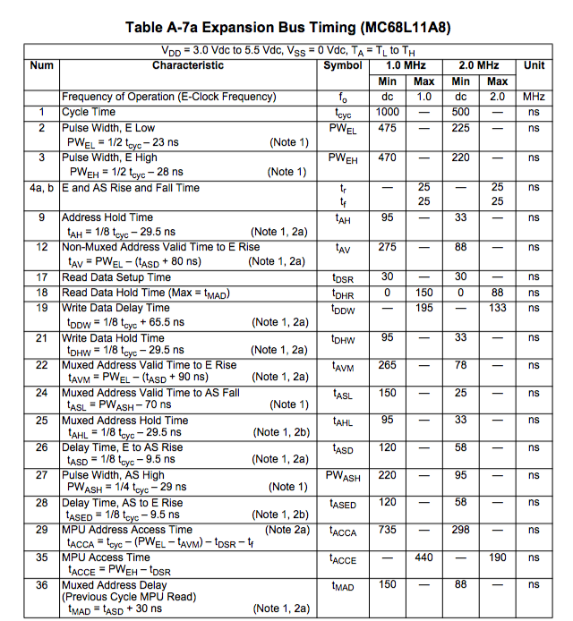 (taken from the 6811 Reference Manual)
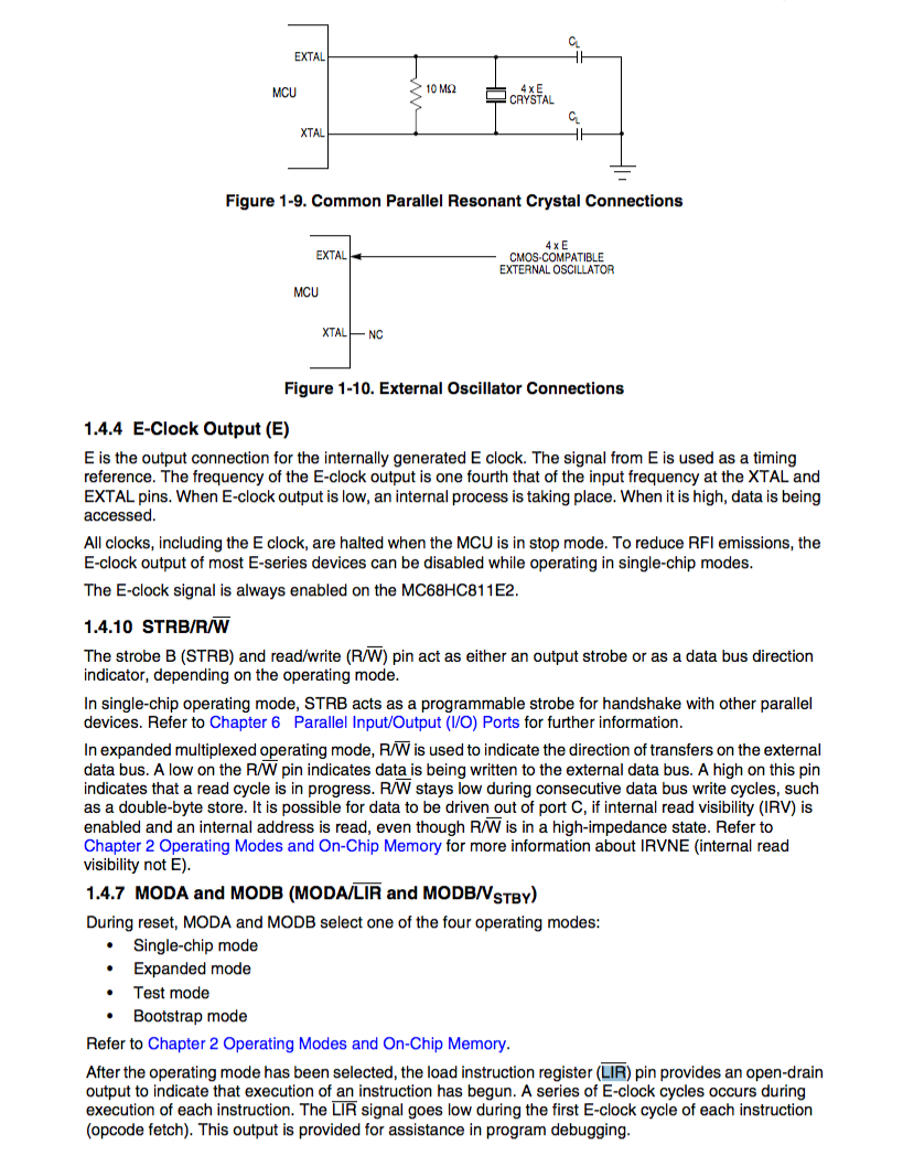
|
| ||||
| Week 11 4/09 |
  if specific CC bit == some predefined value:
        PC = PC + displacement
  else:
        PC = PC + 1
   BEQ, (Branch if equal)
   if  Z bit == 1:
       PC = PC + displacement
   else:
       PC = PC + 1
      LDAA   alpha
      CMPA   #5	      	  ; alpha==5?
      BEQ    same
diff: ...     	      	  ; go here if != 5
      ...
      ...
same: ...     	      	  ; go here if == 5
same: ...                 ; go here if == 5

      LDAA   alpha
      CMPA   #5           ; alpha==5?
      BEQ    same
diff: ...     	      	  ; go here if != 5
      ...
      ...
   0022
+  XXXX
---------
   0005
|
| ||||
| Week 12 4/16 |
|
| ||||
| Week 13 4/23 |
|
| ||||
| Week 14 4/30 |
|
|
Links and Resources
Printing
- How to print a text file (pure ASCII, not an MS Word document) from a beowulf account to the printer @ FH354:
cprint -15 myFile.txt
- How to print a pdf from a beowulf account to the printer @ FH354:
lpr -P ford354 max232.pdf
- How to print an image to the same printer, from a beowulf account:
  convert myImage.jpg  myImage.pdf
  lpr -P ford354 myImage.pdf
Programs
- How to implement AND, OR, NOT and simple logic circuits in Python
- A Python program that generates a truth table.
- A Python program to simulate a simple sequencer.
Software
Demos of Various Circuit
- Hades at U. of Hamburg.
Free Circuit CAD Systems
|
(the video shows an analog circuit, but logic gates are also supported) |
|
PSpice 9
- Pspice 9, Student version. An nice alternative to drawing schematics by hand.
- This is a Windows version. (I have tried to make it work under wine/Mac OS X but haven't been able to make it load the libraries correctly)
- Make sure you select the schematics option when installing the software.
- Select Tools/Schematics when starting the editor
- The schematics editor is located in C:\Program Files\OrCAD_Demo\PSpice\PDesign.exe upon installation.
- Download here!
- PSpice Tutorial
Integrated Circuit Data-Sheets
- Java Applets demonstrating most logical gates
- Texas Instruments and Harris Semiconductors' Data Sheet Search Engine
- Fairchild Semiconductors' Data Sheet Search Engine
- 74LS00, 74LS01, 74LS02, 74LS03, 74LS04, 74LS05, 74LS08, 74LS09, 74LS10, 74LS12, 74LS13, 74LS15, 74LS20, 74LS21, 74LS22, 74LS26, 74LS27, 74LS28, 74LS30, 74LS32, 74LS33, 74LS37, 74LS38, 74LS40, 74LS42, 74LS47, 74LS48, 74LS51, 74LS54, 74LS55, 74LS74, 74LS75, 74LS76, 74LS83, 74LS85, 74LS86, 74LS90, 74LS95, 74LS138, 74HCT240, 74LS243, 74HCT244, 74LS259, 74HCT541
- 9368
- 2114 1Kx4 RAM ( with timing information )
- Octal D-Flipflop (we do not have these chips in our current collection of chips)
Motorola 68HC11 Documentation
- A concise 2-page list of the Instructions and op-codes.
- A good tutorial on 6811 assembly language (pdf)
- 6811 FAQs.
- The official Motorola 68HC11A8 Data Sheet. Fairly cryptic...
- A Motorola 6811 Manual. It is a nicely written refresher on many concepts of assembly language applied to the 6811.
- Check Section 3.2 on addressing modes (inherent, direct, extended, indexed, relative).
- Get a refresher for the different instruction types (arithmetic, shifts, control, etc) in Section 3.4.
- The condition code register is covered in Section 3.5.
- M68HC11 Technical Reference, Motorola
- Section 6.5 shows the instructions in logical groups.
- M68HC11 Pocket Reference.
- Very useful, on Page 15, a list of all the opcodes supported by the 6811, in numerical (hex) order.
- 68HC11A8 Technical Reference: a hardware and engineering description. of the 6811, its ports, and how it operates.
- See Section 10 for a cycle-by-cycle description of the execution of each instruction.
- See Appendix A, Figure A-14 for the timing diagram of a typical (multiplexed expansion) memory access.
- Heathkit ETW3800 Trainer manual (pdf)
- Input/Output with the 6811: Memory-Mapped I/O (Heathkit documentation)
Verilog/CPLD
Books
- Good reference on Verilog: Fundamentals of DIgital Logic with Verilog Design, by Brown & Vranesic, McGraw Hill pub., 2003.
Web Resources
The following links point to good tutorials.
- Verilog Tutorial by Deepak Kumar Tala, 2003.
- Another Verilog Tutorial from Berkeley.
- A tutorial from IBM.
- A very good, concise Verilog Tutorial with many examples by D. K. Blandford, University of Evansville. (pdf)
- Tutorials/Labs on how to create simple combinational and sequential circuits with Xilinx's ISE 13.4.
Xilinx and CPLDs
- CoolRunner2 data sheet and specs.
- Xilinx's extended library of circuits supported, including logic gates and flip-flops.
- Xilinx Tutorial on its ISE.
-
This section is only visible to computers located at Smith College - CSC270 Labs on the CoolRunner II, by Tiffany Liu, Smith College.
